ADS62P49 / ADS62P29
ADS62P48 / ADS62P28
www.ti.com............................................................................................................................................................. SLAS635A–APRIL 2009–REVISED JUNE 2009
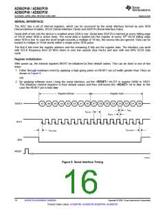
SERIAL INTERFACE TIMING CHARACTERISTICS
Typical values at 25°C, min and max values across the full temperature range TMIN = –40°C to TMAX = 85°C, AVDD = 3.3V,
DRVDD = 1.8V (unless otherwise noted).
PARAMETER
SCLK frequency (= 1/ tSCLK
MIN
> DC
25
TYP
MAX
UNIT
MHz
ns
fSCLK
tSLOADS
tSLOADH
tDS
)
20
SEN to SCLK setup time
SCLK to SEN hold time
SDATA setup time
25
ns
25
ns
tDH
SDATA hold time
25
ns
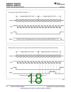
Serial Register Readout
The device includes an option where the contents of the internal registers can be read back. This may be useful
as a diagnostic check to verify the serial interface communication between the external controller AND the ADC.
a. First, set register bit <SERIAL READOUT> = 1. This also disables any further writes into the registers.
b. Initiate a serial interface cycle specifying the address of the register (A7-A0) whose content has to be read.
c. The device outputs the contents (D7-D0) of the selected register on the SDOUT pin (64).
d. The external controller can latch the contents at the falling edge of SCLK.
e. To enable register writes, reset register bit <SERIAL READOUT> = 0. SDOUT is a CMOS output pin; the readout functionality is
available whether the ADC output data interface is LVDS or CMOS.
When <SERIAL READOUT> is disabled, the SDOUT pin is forced low by the device (and not put in
high-impedance). If serial readout is not used, the SDOUT pin has to be floated.
Copyright © 2009, Texas Instruments Incorporated
Submit Documentation Feedback
17
Product Folder Link(s): ADS62P49 / ADS62P29 ADS62P48 / ADS62P28

 TI [ TEXAS INSTRUMENTS ]