ADS62P49 / ADS62P29
ADS62P48 / ADS62P28
SLAS635A–APRIL 2009–REVISED JUNE 2009............................................................................................................................................................. www.ti.com
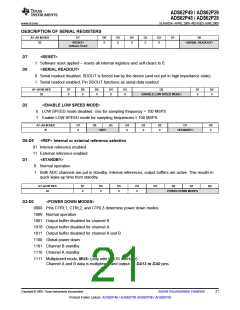
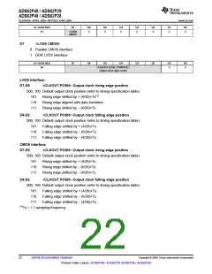
A7–A0 IN HEX
41
D7
D6
D5
D4
D3
D2
D1
D0
<LVDS
0
0
0
0
0
0
0
CMOS>
D7
<LVDS CMOS>
0
1
Parallel CMOS interface
DDR LVDS interface
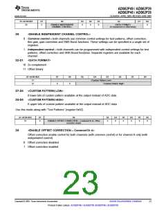
A7–A0 IN HEX
44
D7
D6
D5
D4
D3
D2
D1
D0
<CLKOUT EDGE CONTROL>
0
0
Output clock edge control
LVDS interface
D7-D5 <CLKOUT POSN> Output clock rising edge position
000, 100 Default output clock position (refer to timing specification table)
101
110
111
Rising edge shifted by + (4/26)×Ts(1)
Rising edge aligned with data transition
Rising edge shifted by – (4/26)×Ts
D4-D2
<CLKOUT POSN> Output clock falling edge position
000, 100 Default output clock position (refer to timing specification table)
101
110
111
Falling edge shifted by + (4/26)×Ts
Falling edge shifted by – (6/26)×Ts
Falling edge shifted by – (4/26)×Ts
CMOS interface
D7-D5
<CLKOUT POSN> Output clock rising edge position
000, 100 Default output clock position (refer to timing specification table)
101
110
111
Rising edge shifted by + (4/26)×Ts
Rising edge shifted by – (6/26)×Ts
Rising edge shifted by – (4/26)×Ts
D4-D2
<CLKOUT POSN> Output clock falling edge position
000, 100 Default output clock position (refer to timing specification table)
101
110
111
Falling edge shifted by + (4/26)×Ts
Falling edge shifted by – (6/26)×Ts
Falling edge shifted by – (4/26)×Ts
(1)Ts = 1 / sampling frequency
22
Submit Documentation Feedback
Copyright © 2009, Texas Instruments Incorporated
Product Folder Link(s): ADS62P49 / ADS62P29 ADS62P48 / ADS62P28

 TI [ TEXAS INSTRUMENTS ]