ADS62P49 / ADS62P29
ADS62P48 / ADS62P28
SLAS635A–APRIL 2009–REVISED JUNE 2009............................................................................................................................................................. www.ti.com
DEVICE CONFIGURATION
ADS62Px9/x8 can be configured independently using either parallel interface control or serial interface
programming.
PARALLEL CONFIGURATION ONLY
To put the device in parallel configuration mode, keep RESET tied to high (AVDD).
Now, pins SEN, SCLK, CTRL1, CTRL2 and CTRL3 can be used to directly control certain modes of the ADC.
The device can be easily configured by connecting the parallel pins to the correct voltage levels (as described in
Table 3 to Table 6). There is no need to apply reset and SDATA pin can be connected to ground..
In this mode, SEN and SCLK function as parallel interface control pins. Frequently used functions can be
controlled in this mode – Power down modes, internal/external reference, selection between LVDS/CMOS
interface and output data format.
Table 3 has a brief description of the modes controlled by the four parallel pins.
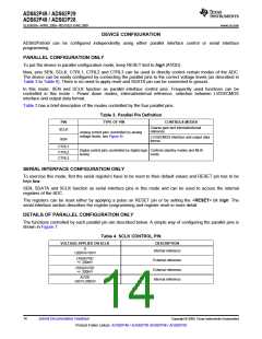
Table 3. Parallel Pin Definition
PIN
TYPE OF PIN
CONTROLS MODES
Coarse gain and internal/external
reference
SCLK
Analog control pins (controlled by analog
voltage levels, see Figure 8)
LVDS/CMOS interface and output data
format
SEN
CTRL1
CTRL2
CTRL3
Digital control pins (controlled by digital logic Controls standby modes and MUX
levels) mode.
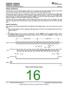
SERIAL INTERFACE CONFIGURATION ONLY
To exercise this mode, first the serial registers have to be reset to their default values and RESET pin has to be
kept low.
SEN, SDATA and SCLK function as serial interface pins in this mode and can be used to access the internal
registers of the ADC.
The registers can be reset either by applying a pulse on RESET pin or by setting the <RESET> bit high. The
serial interface section describes the register programming and register reset in more detail
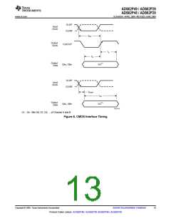
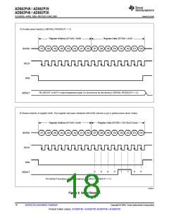
DETAILS OF PARALLEL CONFIGURATION ONLY
The functions controlled by each parallel pin are described below. A simple way of configuring the parallel pins is
shown in Figure 7.
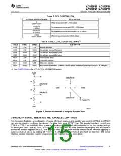
Table 4. SCLK CONTROL PIN
VOLTAGE APPLIED ON SCLK
DESCRIPTION
0
Internal reference
+200mV/-0mV
(3/8)AVDD
+/- 200mV
External reference
External reference
Internal reference
(5/8)2AVDD
+/- 200mV
AVDD
+0mV/-200mV
14
Submit Documentation Feedback
Copyright © 2009, Texas Instruments Incorporated
Product Folder Link(s): ADS62P49 / ADS62P29 ADS62P48 / ADS62P28

 TI [ TEXAS INSTRUMENTS ]