ADS62P49 / ADS62P29
ADS62P48 / ADS62P28
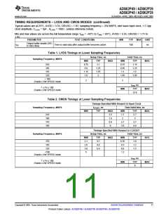
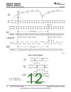
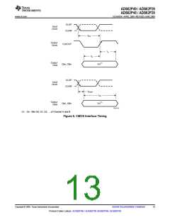
www.ti.com............................................................................................................................................................. SLAS635A–APRIL 2009–REVISED JUNE 2009
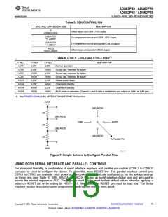
Table 5. SEN CONTROL PIN
VOLTAGE APPLIED ON SEN
DESCRIPTION
0
Offset binary and DDR LVDS output
+200mV/-0mV
(3/8)AVDD
+/- 200mV
2’s complement format and DDR LVDS output
2’s complement format and parallel CMOS output
Offset binary and parallel CMOS output
(5/8)AVDD
+/- 200mV
AVDD
+0mV/-200mV
Table 6. CTRL1, CTRL2 and CTRL3 PINS(1)
CTRL1
LOW
LOW
LOW
LOW
HIGH
HIGH
HIGH
HIGH
CTRL2
LOW
LOW
HIGH
HIGH
LOW
LOW
HIGH
HIGH
CTRL3
LOW
HIGH
LOW
HIGH
LOW
HIGH
LOW
HIGH
DESCRIPTION
Normal operation
Do not use, reserved for future
Do not use, reserved for future
Do not use, reserved for future
Global power down
Channel B standby
Channel A standby
MUX mode of operation, Channel A and B data is multiplexed and output on DA13 to DA0 pins.
(1) See POWER DOWN in the APPLICATION INFORMATION section.
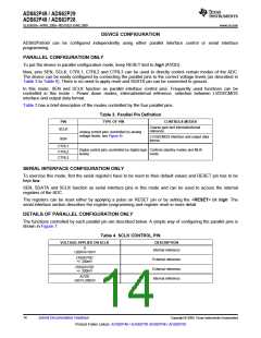
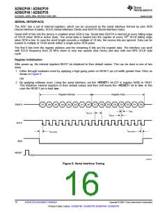
AVDD
(5/8) AVDD
3R
(5/8) AVDD
GND
AVDD
2R
(3/8) AVDD
(3/8) AVDD
3R
To Parallel Pin
GND
S0321-01
Figure 7. Simple Scheme to Configure Parallel Pins
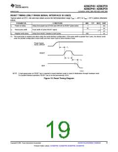
USING BOTH SERIAL INTERFACE AND PARALLEL CONTROLS
For increased flexibility, a combination of serial interface registers and parallel pin controls (CTRL1 to CTRL3)
can also be used to configure the device. To allow this, keep RESET low. The parallel interface control pins
CTRL1 to CTRL3 are available. After power-up, the device is automatically configured as per the voltage settings
on these pins (see Table 6). SEN, SDATA, and SCLK function as serial interface digital pins and are used to
access the internal registers of ADC. The registers must first be reset to their default values either by applying a
pulse on RESET pin or by setting bit <RST> = 1. After reset, the RESET pin must be kept low. The Serial
Interface section describes register programming and register reset in more detail.
Copyright © 2009, Texas Instruments Incorporated
Submit Documentation Feedback
15
Product Folder Link(s): ADS62P49 / ADS62P29 ADS62P48 / ADS62P28

 TI [ TEXAS INSTRUMENTS ]