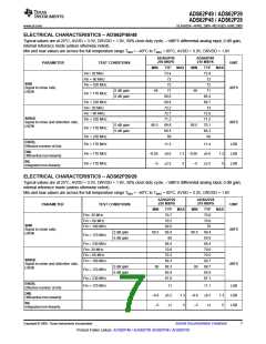
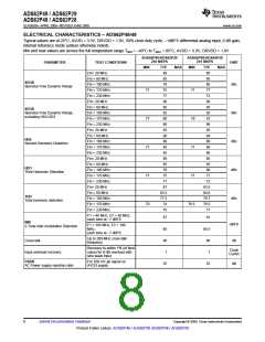
ADS62P49 / ADS62P29
ADS62P48 / ADS62P28
www.ti.com............................................................................................................................................................. SLAS635A–APRIL 2009–REVISED JUNE 2009
TIMING REQUIREMENTS – LVDS AND CMOS MODES (continued)
Typical values are at 25°C, AVDD = 3.3V, DRVDD = 1.8V, sampling frequency = 250 MSPS, sine wave input clock, 1.5 Vpp
clock amplitude, CLOAD = 5pF , RLOAD = 100Ω , (unless otherwise noted).
Min and max values are across the full temperature range TMIN = –40°C to TMAX = 85°C, AVDD = 3.3V, DRVDD = 1.7V to
1.9V
PARAMETER
TEST CONDITIONS
MIN
TYP
MAX
UNIT
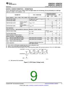
Output buffer enable (OE)
to data delay
tOE
Time to valid data after output buffer becomes active
100
ns
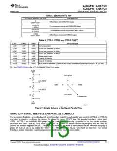
Table 1. LVDS Timings at Lower Sampling Frequencies
Setup Time, ns
Hold Time, ns
Sampling Frequency, MSPS
MIN
0.75
0.9
TYP
1.1
MAX
MIN
0.75
0.85
1.1
TYP
1.15
1.25
1.5
MAX
210
185
153
125
1.25
1.55
2
1.15
1.6
1.45
1.85
< 100
2
2
Enable LOW SPEED mode
tPDI, ns
TYP
1 ≤ Fs ≤ 100
Enable LOW SPEED mode
MIN
MAX
12.6
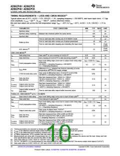
Table 2. CMOS Timings at Lower Sampling Frequencies
Timings Specified With Respect to Input Clock
Sampling Frequency, MSPS
tSTART, ns
TYP
Data Valid time, ns
MIN
MAX
2.5
1.9
0.9
6
MIN
1.7
2
TYP
2.7
3
MAX
210
190
170
150
2.7
3.6
3.7
4.6
Timings Specified With Respect to CLKOUT
Sampling Frequency, MSPS
Setup Time, ns
Hold Time, ns
MIN
2.1
2.8
3.8
5
TYP
3.7
4.4
5.4
MAX
MIN
0.35
0.5
TYP
1.0
1.2
1.5
MAX
170
150
125
0.8
<100
1.2
Enable LOW SPEED mode
tPDI, ns
TYP
9
1 ≤ Fs ≤ 100
Enable LOW SPEED mode
MIN
MAX
Copyright © 2009, Texas Instruments Incorporated
Submit Documentation Feedback
11
Product Folder Link(s): ADS62P49 / ADS62P29 ADS62P48 / ADS62P28

 TI [ TEXAS INSTRUMENTS ]