ADS1291
ADS1292
ADS1292R
SBAS502A –DECEMBER 2011–REVISED MARCH 2012
www.ti.com
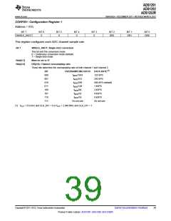
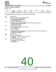
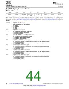
CONFIG2: Configuration Register 2
Address = 02h
BIT 7
1
BIT 6
BIT 5
BIT 4
BIT 3
BIT 2
0
BIT 1
BIT 0
PDB_LOFF_
COMP
PDB_REFBUF
VREF_4V
CLK_EN
INT_TEST
TEST_FREQ
This register configures the test signal, clock, reference, and LOFF buffer.
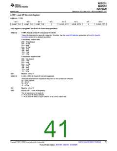
Bit 7
Bit 6
Must be set to '1'
PDB_LOFF_COMP: Lead-off comparator power-down
This bit powers down the lead-off comparators.
0 = Lead-off comparators disabled (default)
1 = Lead-off comparators enabled
Bit 5
Bit 4
Bit 3
PDB_REFBUF: Reference buffer power-down
This bit powers down the internal reference buffer so that the external reference can be used.
0 = Reference buffer is powered down (default)
1 = Reference buffer is enabled
VREF_4V: Enables 4-V reference
This bit chooses between 2.42-V and 4.033-V reference.
0 = 2.42-V reference (default)
1 = 4.033-V reference
CLK_EN: CLK connection
This bit determines if the internal oscillator signal is connected to the CLK pin when an internal oscillator is used.
0 = Oscillator clock output disabled (default)
1 = Oscillator clock output enabled
Bit 2
Bit 1
Must be set to '0'
INT_TEST: Test signal selection
This bit determines whether the test signal is turned on or off.
0 = Off (default)
1 = On; amplitude = ±(VREFP – VREFN)/2400
Bit 0
TEST_FREQ: Test signal frequency
This bit determines the test signal frequency.
0 = At dc (default)
1 = Square wave at 1 Hz
40
Submit Documentation Feedback
Copyright © 2011–2012, Texas Instruments Incorporated
Product Folder Link(s): ADS1291 ADS1292 ADS1292R

 TI [ TEXAS INSTRUMENTS ]