ADS1291
ADS1292
ADS1292R
www.ti.com
SBAS502A –DECEMBER 2011–REVISED MARCH 2012
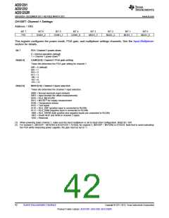
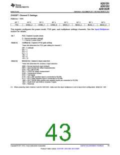
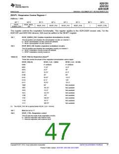
CH2SET: Channel 2 Settings
Address = 05h
BIT 7
PD2
BIT 6
BIT 5
BIT 4
BIT 3
BIT 2
BIT 1
BIT 0
GAIN2_2
GAIN2_1
GAIN2_0
MUX2_3
MUX2_2
MUX2_1
MUX2_0
This register configures the power mode, PGA gain, and multiplexer settings channels. See the Input Multiplexer
section for details.
Bit 7
PD2: Channel 2 power-down
0 = Normal operation (default)
1 = Channel 2 power-down(1)
Bits[6:4]
GAIN2[2:0]: Channel 2 PGA gain setting
These bits determine the PGA gain setting for channel 2.
000 = 6 (default)
001 = 1
010 = 2
011 = 3
100 = 4
101 = 8
110 = 12
Bits[3:0]
MUX2[3:0]: Channel 2 input selection
These bits determine the channel 2 input selection.
0000 = Normal electrode input (default)
0001 = Input shorted (for offset measurements)
0010 = RLD_MEASURE
0011 = VDD/2 for supply measurement
0100 = Temperature sensor
0101 = Test signal
0110 = RLD_DRP (positive input is connected to RLDIN)
0111 = RLD_DRM (negative input is connected to RLDIN)
1000 = RLD_DRPM (both positive and negative inputs are connected to RLDIN)
1001 = Route IN3P and IN3N to channel 2 inputs
1010 = Reserved
(1) When powering down channel 2 and for ADS1291, make sure the input multiplexer is set to input short configuration. Bits[3:0] = 001.
Copyright © 2011–2012, Texas Instruments Incorporated
Submit Documentation Feedback
43
Product Folder Link(s): ADS1291 ADS1292 ADS1292R

 TI [ TEXAS INSTRUMENTS ]