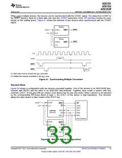
ADS1291
ADS1292
ADS1292R
www.ti.com
SBAS502A –DECEMBER 2011–REVISED MARCH 2012
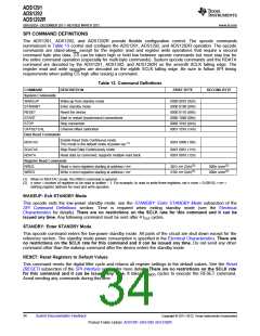
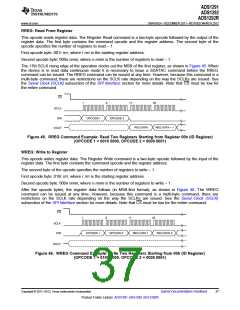
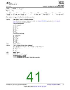
RREG: Read From Register
This opcode reads register data. The Register Read command is a two-byte opcode followed by the output of the
register data. The first byte contains the command opcode and the register address. The second byte of the
opcode specifies the number of registers to read – 1.
First opcode byte: 001r rrrr, where r rrrr is the starting register address.
Second opcode byte: 000n nnnn, where n nnnn is the number of registers to read – 1.
The 17th SCLK rising edge of the operation clocks out the MSB of the first register, as shown in Figure 45. When
the device is in read data continuous mode it is necessary to issue a SDATAC command before the RREG
command can be issued. The RREG command can be issued at any time. However, because this command is a
multi-byte command, there are restrictions on the SCLK rate depending on the way the SCLKs are issued. See
the Serial Clock (SCLK) subsection of the SPI Interface section for more details. Note that CS must be low for
the entire command.
CS
1
9
17
25
SCLK
DIN
OPCODE 1
OPCODE 2
REG DATA
REG DATA + 1
DOUT
Figure 45. RREG Command Example: Read Two Registers Starting from Register 00h (ID Register)
(OPCODE 1 = 0010 0000, OPCODE 2 = 0000 0001)
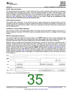
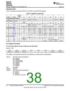
WREG: Write to Register
This opcode writes register data. The Register Write command is a two-byte opcode followed by the input of the
register data. The first byte contains the command opcode and the register address.
The second byte of the opcode specifies the number of registers to write – 1.
First opcode byte: 010r rrrr, where r rrrr is the starting register address.
Second opcode byte: 000n nnnn, where n nnnn is the number of registers to write – 1.
After the opcode bytes, the register data follows (in MSB-first format), as shown in Figure 46. The WREG
command can be issued at any time. However, because this command is a multi-byte command, there are
restrictions on the SCLK rate depending on the way the SCLKs are issued. See the Serial Clock (SCLK)
subsection of the SPI Interface section for more details. Note that CS must be low for the entire command.
CS
1
9
17
25
SCLK
DIN
OPCODE 1
OPCODE 2
REG DATA 1
REG DATA 2
DOUT
Figure 46. WREG Command Example: Write Two Registers Starting from 00h (ID Register)
(OPCODE 1 = 0100 0000, OPCODE 2 = 0000 0001)
Copyright © 2011–2012, Texas Instruments Incorporated
Submit Documentation Feedback
37
Product Folder Link(s): ADS1291 ADS1292 ADS1292R

 TI [ TEXAS INSTRUMENTS ]