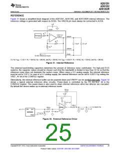
ADS1291
ADS1292
ADS1292R
www.ti.com
SBAS502A –DECEMBER 2011–REVISED MARCH 2012
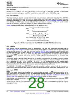
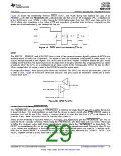
Figure 35 shows the relationship between DRDY, DOUT, and SCLK during data retrieval (in case of an
ADS1291, ADS1292, and ADS1292R with a selected data rate that gives 24-bit resolution). DOUT is latched out
at the SCLK rising edge. DRDY is pulled high at the SCLK falling edge. Note that DRDY goes high on the first
SCLK falling edge regardless of the status of CS and regardless of whether data are being retrieved from the
device or a command is being sent through the DIN pin.
DRDY
DOUT
SCLK
Bit 71
Bit 70
Bit 69
Figure 35. DRDY with Data Retrieval (CS = 0)
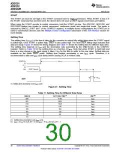
GPIO
The ADS1291, ADS1292, and ADS1292R have a total of two general-purpose digital input/output (GPIO) pins
available in the normal mode of operation. The digital I/O pins are individually configurable as either inputs or as
outputs through the GPIOC bits register. The GPIOD bits in the GPIO register control the level of the pins. When
reading the GPIOD bits, the data returned are the logic level of the pins, whether they are programmed as inputs
or outputs. When the GPIO pin is configured as an input, a write to the corresponding GPIOD bit has no effect.
When configured as an output, a write to the GPIOD bit sets the output value.
If configured as inputs, these pins must be driven (do not float). The GPIO pins are set as inputs after power-on
or after a reset. Figure 36 shows the GPIO port structure. The pins should be shorted to DGND with a series
resistor if not used.
GPIO Data (read)
GPIO Pin
GPIO Data (write)
GPIO Control
Figure 36. GPIO Port Pin
Power-Down and Reset (PWDN/RESET)
The PWDN/RESET pins are shared. If PWDN/RESET is held low for longer than 29 fMOD clock cycles, the device
is powered down. The implementation is such that the device is always reset when PWDN/RESET makes a
transition from high to low. If the device is powered down it is reset first and then if 210 clock elapses it is
powered down. Hence, all registers must be rewritten after power up.
There are two methods to reset the ADS1291, ADS1292, and ADS1292R: pull the PWDN/RESET pin low, or
send the RESET opcode command. When using the PWDN/RESET pin, take it low to force a reset. Make sure
to follow the minimum pulse width timing specifications before taking the PWDN/RESET pin back high. The
RESET command takes effect on the eighth SCLK falling edge of the opcode command. On reset it takes 18 tCLK
cycles to complete initialization of the configuration registers to the default states and start the conversion cycle.
Note that an internal RESET is automatically issued to the digital filter whenever the CONFIG1, RESP1, and
RESP2 registers are set to a new value with a WREG command.
Copyright © 2011–2012, Texas Instruments Incorporated
Submit Documentation Feedback
29
Product Folder Link(s): ADS1291 ADS1292 ADS1292R

 TI [ TEXAS INSTRUMENTS ]