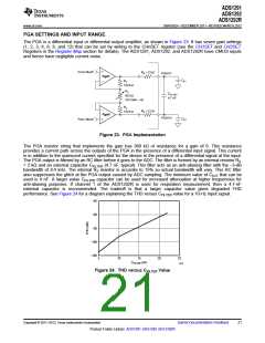
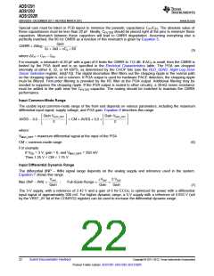
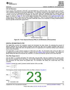
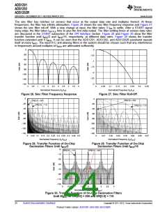
ADS1291
ADS1292
ADS1292R
www.ti.com
SBAS502A –DECEMBER 2011–REVISED MARCH 2012
REFERENCE
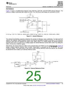
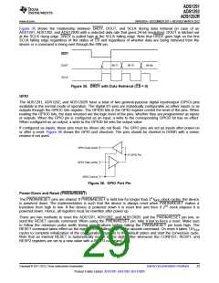
Figure 31 shows a simplified block diagram of the ADS1291, ADS1292, and ADS1292R internal reference. The
reference voltage is generated with respect to AVSS. The VREFN pin must always be connected to AVSS.
1 mF
VCAP1
(1)
R1
2.42 V or
4.033 V
Bandgap
VREFP
(1)
R3
10 mF
0.1 mF
(1)
R2
VREFN
AVSS
To ADC Reference Inputs
(1) For VREF = 2.42 V: R1 = 100 kΩ, R2 = 200 kΩ, and R3 = 200 kΩ. For VREF = 4.033 V: R1 = 84 kΩ, R2 = 120 kΩ, and R3 = 280 kΩ.
Figure 31. Internal Reference
The external band-limiting capacitors determine the amount of reference noise contribution. For high-end ECG
systems, the capacitor values should be chosen such that the bandwidth is limited to less than 10 Hz so that the
reference noise does not dominate the system noise. When using a 3-V analog supply, the internal reference
must be set to 2.42 V. In case of a 5-V analog supply, the internal reference can be set to 4.033 V by setting the
VREF_4V bit in the CONFIG2 register.
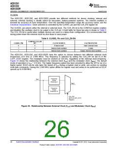
Alternatively, the internal reference buffer can be powered down and VREFP can be applied externally. Figure 32
shows a typical external reference drive circuitry. Power-down is controlled by the PD_REFBUF bit in the
CONFIG2 register. This power-down is also used to share internal references when two devices are cascaded.
By default the device wakes up in external reference mode.
100 kW
10 pF
+5 V
0.1 mF
100 W
To VREFP Pin
OPA211
100 W
22 mF
10 mF
0.1 mF
+5 V
VIN
REF5025
TRIM
OUT
100 mF
22 mF
Figure 32. External Reference Driver
Copyright © 2011–2012, Texas Instruments Incorporated
Submit Documentation Feedback
25
Product Folder Link(s): ADS1291 ADS1292 ADS1292R

 TI [ TEXAS INSTRUMENTS ]