ADS1299
SBAS499A –JULY 2012–REVISED AUGUST 2012
www.ti.com
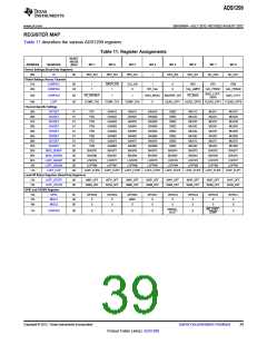
User Register Description
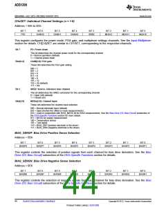
ID: ID Control Register (Factory-Programmed, Read-Only)
Address = 00h
BIT 7
BIT 6
BIT 5
BIT 4
1
BIT 3
BIT 2
BIT 1
BIT 0
REV_ID3
REV_ID2
REV_ID1
DEV_ID2
DEV_ID1
NU_CH2
NU_CH1
This register is programmed during device manufacture to indicate device characteristics.
Bits[7:5]
Bit 4
Not used
Must be set to '1'
Bits[3:0]
Factory-programmed device identification bits
1110 = ADS1299
CONFIG1: Configuration Register 1
Address = 01h
BIT 7
1
BIT 6
BIT 5
BIT 4
1
BIT 3
0
BIT 2
DR2
BIT 1
DR1
BIT 0
DR0
DAISY_EN
CLK_EN
This register configures the DAISY_EN bit, clock, and data rate.
Bit 7
Bit 6
Must be set to '1'
DAISY_EN: Daisy-chain and multiple readback mode
This bit determines which mode is enabled.
0 = Daisy-chain mode (default)
1 = Multiple readback mode
Bit 5
CLK_EN: CLK connection(1)
This bit determines if the internal oscillator signal is connected to the CLK pin when the CLKSEL pin = 1.
0 = Oscillator clock output disabled (default)
1 = Oscillator clock output enabled
Bits[4:3]
Bits[2:0]
Must always be set to '10'
DR[2:0]: Output data rate
fMOD = fCLK / 2.
These bits determine the output data rate of the device.
(1) Additional power is consumed when driving external devices.
BIT
000
DATA RATE
SAMPLE RATE(1)
16 kSPS
8 kSPS
fMOD / 64
fMOD / 128
fMOD / 256
fMOD / 512
fMOD / 1024
fMOD / 2048
fMOD / 4096
Do not use
001
010
4 kSPS
011
2 kSPS
100
1 kSPS
101
500 SPS
250 SPS
n/a
110 (default)
111
(1) fCLK = 2.048 MHz.
40
Submit Documentation Feedback
Copyright © 2012, Texas Instruments Incorporated
Product Folder Link(s): ADS1299

 TI [ TEXAS INSTRUMENTS ]