ADS1299
www.ti.com
SBAS499A –JULY 2012–REVISED AUGUST 2012
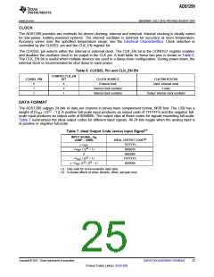
CLOCK
The ADS1299 provides two methods for device clocking: internal and external. Internal clocking is ideally suited
for low-power, battery-powered systems. The internal oscillator is trimmed for accuracy at room temperature.
Accuracy varies over the specified temperature range; see the Electrical Characteristics. Clock selection is
controlled by the CLKSEL pin and the CLK_EN register bit.
The CLKSEL pin selects either the internal or external clock. The CLK_EN bit in the CONFIG1 register enables
and disables the oscillator clock to be output in the CLK pin. A truth table for these two pins is shown in Table 6.
The CLK_EN bit is useful when multiple devices are used in a daisy-chain configuration. During power-down, the
external clock is recommended be shut down to save power.
Table 6. CLKSEL Pin and CLK_EN Bit
CONFIG1.CLK_EN
CLKSEL PIN
BIT
CLOCK SOURCE
External clock
CLK PIN STATUS
Input: external clock
3-state
0
1
1
X
0
Internal clock oscillator
Internal clock oscillator
1
Output: internal clock oscillator
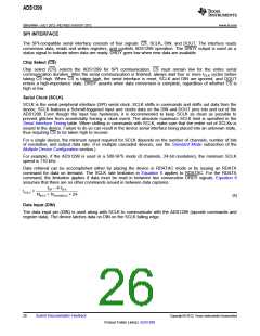
DATA FORMAT
The ADS1299 outputs 24 bits of data per channel in binary twos complement format, MSB first. The LSB has a
weight of [VREF / (223 – 1)]. A positive full-scale input produces an output code of 7FFFFFh and the negative full-
scale input produces an output code of 800000h. The output clips at these codes for signals exceeding full-scale.
Table 7 summarizes the ideal output codes for different input signals. All 24 bits toggle when the analog input is
at positive or negative full-scale.
Table 7. Ideal Output Code versus Input Signal(1)
INPUT SIGNAL, VIN
(AINP – AINN)
IDEAL OUTPUT CODE(2)
7FFFFFh
≥ VREF
+VREF / (223 – 1)
0
000001h
000000h
–VREF / (223 – 1)
≤ –VREF (223 / 223 – 1)
FFFFFFh
800000h
(1) Only valid for 24-bit resolution data rates.
(2) Excludes effects of noise, linearity, offset, and gain error.
Copyright © 2012, Texas Instruments Incorporated
Submit Documentation Feedback
25
Product Folder Link(s): ADS1299

 TI [ TEXAS INSTRUMENTS ]