ADS1299
SBAS499A –JULY 2012–REVISED AUGUST 2012
www.ti.com
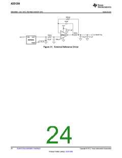
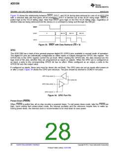
Figure 33 shows the relationship between DRDY, DOUT, and SCLK during data retrieval (in case of an ADS1299
with a selected data rate that gives 24-bit resolution). DOUT is latched out at the SCLK rising edge. DRDY is
pulled high at the SCLK falling edge. Note that DRDY goes high on the first SCLK falling edge, regardless of
whether data are being retrieved from the device or a command is being sent through the DIN pin.
DRDY
DOUT
SCLK
X
Bit 215
Bit 214
Bit 213
Figure 33. DRDY with Data Retrieval (CS = 0)
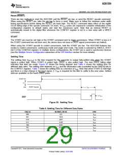
GPIO
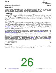
The ADS1299 has a total of four general-purpose digital I/O (GPIO) pins available in normal mode of operation.
The digital I/O pins are individually configurable as either inputs or outputs through the GPIOC bits register. The
GPIOD bits in the GPIO register control the pin level. When reading the GPIOD bits, the data returned are the
logic level of the pins, whether they are programmed as inputs or outputs. When the GPIO pin is configured as
an input, a write to the corresponding GPIOD bit has no effect. When configured as an output, a write to the
GPIOD bit sets the output value.
If configured as inputs, these pins must be driven (do not float). The GPIO pins are set as inputs after power-on
or after a reset. Figure 34 shows the GPIO port structure. The pins should be shorted to DGND if not used.
GPIO Data (read)
GPIO Pin
GPIO Data (write)
GPIO Control
Figure 34. GPIO Port Pin
Power-Down (PWDN)
When PWDN is pulled low, all on-chip circuitry is powered down. To exit power-down mode, take the PWDN pin
high. Upon exiting from power-down mode, the internal oscillator and the reference require time to wake up.
During power-down, the external clock is recommended to be shut down to save power.
28
Submit Documentation Feedback
Copyright © 2012, Texas Instruments Incorporated
Product Folder Link(s): ADS1299

 TI [ TEXAS INSTRUMENTS ]