ADS1299
www.ti.com
SBAS499A –JULY 2012–REVISED AUGUST 2012
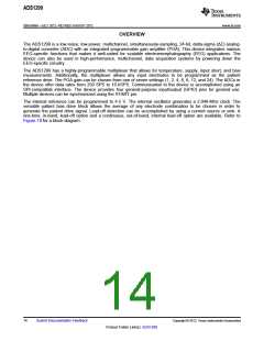
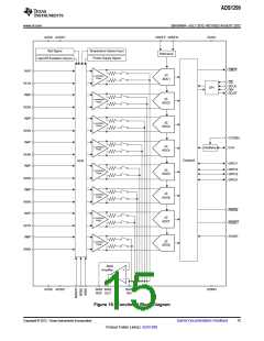
AVDD AVDD1
Test Signal
VREFP VREFN
DVDD
Temperature Sensor Input
Power-Supply Signal
Reference
Lead-Off Excitation Source
DRDY
IN1P
DS
Low-Noise
PGA1
ADC1
CS
IN1N
IN2P
SCLK
DIN
DOUT
SPI
DS
Low-Noise
PGA2
ADC2
IN2N
IN3P
DS
Low-Noise
PGA3
ADC3
IN3N
IN4P
CLKSEL
CLK
DS
Low-Noise
PGA4
Oscillator
ADC4
IN4N
IN5P
Control
MUX
GPIO1
GPIO4
GPIO3
DS
Low-Noise
PGA5
ADC5
IN5N
IN6P
GPIO2
DS
Low-Noise
PGA6
ADC6
IN6N
IN7P
PWDN
RESET
DS
Low-Noise
PGA7
ADC7
IN7N
IN8P
START
DS
Low-Noise
PGA8
ADC8
IN8N
BIAS
Amplifier
AVSS AVSS1
DGND
BIAS BIAS
REF OUT
BIAS
INV
Figure 18. Functional Block Diagram
Copyright © 2012, Texas Instruments Incorporated
Submit Documentation Feedback
15
Product Folder Link(s): ADS1299

 TI [ TEXAS INSTRUMENTS ]