ADS1115-Q1
www.ti.com
SBAS563 –DECEMBER 2011
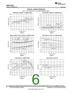
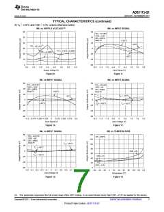
TYPICAL CHARACTERISTICS (continued)
At TA = +25°C and VDD = 3.3V, unless otherwise noted.
INL vs SUPPLY VOLTAGE(2)
INL vs INPUT SIGNAL
60
60
40
FS = ±2.048V
VDD = 3.3V
DR = 8SPS
Best Fit
50
40
+125°C
20
-40°C
FS = ±6.144V(1)
30
0
FS = ±0.512, ±0.256V
FS = ±2.048V
20
10
0
-20
-40
-60
+25°C
2.0
2.5
3.0
3.5
4.0
4.5
5.0
5.5
-2.0 -1.5 -1.0 -0.5
0
0.5
1.0
1.5
2.0
Supply Voltage (V)
Input Signal (V)
Figure 8.
Figure 9.
INL vs INPUT SIGNAL
INL vs INPUT SIGNAL
60
40
60
40
FS = ±0.512V
VDD = 3.3V
DR = 8SPS
Best Fit
FS = ±2.048V
VDD = 5V
DR = 8SPS
Best Fit
+125°C
20
20
TA = -40°C
-40°C
0
0
+25°C
TA = +125°C
TA = +25°C
-20
-40
-60
-20
-40
-60
-0.5 -0.375 -0.250 -0.125
0
0.125 0.250 0.375 0.5
-2.0 -1.5 -1.0 -0.5
0
0.5
1.0
1.5
2.0
Input Signal (V)
Input Voltage (V)
Figure 10.
Figure 11.
INL vs INPUT SIGNAL
INL vs TEMPERATURE
60
40
140
120
100
80
FS = ±0.512V
VDD = 5V
DR = 8SPS
Best Fit
DR = 8SPS
TA = +25°C
20
TA = -40°C
0
VDD = 2V
60
TA = +125°C
VDD = 5V
-20
-40
-60
40
20
VDD = 3.3V
0
-0.5 -0.4 -0.3 -0.2 -0.1
0
0.1 0.2 0.3 0.4 0.5
-60 -40 -20
0
20
40
60
80 100 120 140
Input Voltage (V)
Temperature (°C)
Figure 12.
Figure 13.
(2) This parameter expresses the full-scale range of the ADC scaling. In no event should more than VDD + 0.3V be applied to this device.
Submit Documentation Feedback
Copyright © 2011, Texas Instruments Incorporated
7
Product Folder Link(s) :ADS1115-Q1

 TI [ TEXAS INSTRUMENTS ]