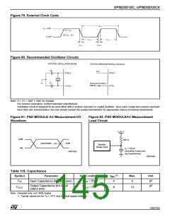
UPSD3212C, UPSD3212CV
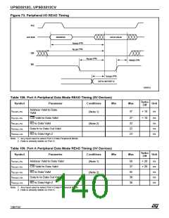
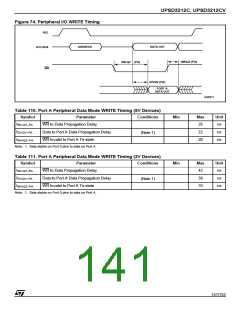
Figure 74. Peripheral I/O WRITE Timing
ALE
ADDRESS
DATA OUT
A/D BUS
tWHQZ (PA)
tWLQV (PA)
WR
tDVQV (PA)
PORT A
DATA OUT
AI06611
Table 110. Port A Peripheral Data Mode WRITE Timing (5V Devices)
Symbol
WLQV–PA
DVQV–PA
WHQZ–PA
Parameter
WR to Data Propagation Delay
Data to Port A Data Propagation Delay
WR Invalid to Port A Tri-state
Conditions
Min
Max
25
Unit
ns
t
t
t
22
ns
(Note 1)
20
ns
Note: 1. Data stable on Port 0 pins to data on Port A.
Table 111. Port A Peripheral Data Mode WRITE Timing (3V Devices)
Symbol
WLQV–PA
DVQV–PA
WHQZ–PA
Parameter
WR to Data Propagation Delay
Data to Port A Data Propagation Delay
WR Invalid to Port A Tri-state
Conditions
Min
Max
42
Unit
ns
t
t
t
38
ns
(Note 1)
33
ns
Note: 1. Data stable on Port 0 pins to data on Port A.
141/152

 STMICROELECTRONICS [ ST ]