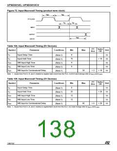
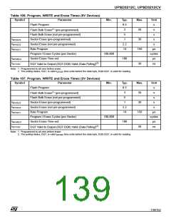
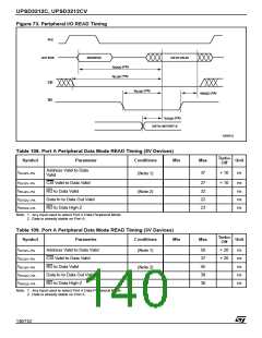
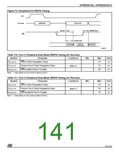
UPSD3212C, UPSD3212CV
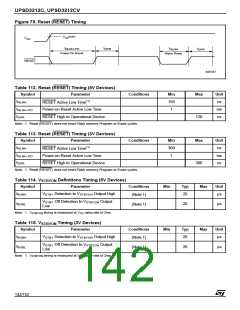
Figure 75. Reset (RESET) Timing
VCC(min)
V
CC
t
t
OPR
t
t
NLNH-PO
NLNH
OPR
Power-On Reset
Warm Reset
RESET
AI07437
Table 112. Reset (RESET) Timing (5V Devices)
Symbol
Parameter
Conditions
Min
150
1
Max
Unit
(1)
t
t
t
ns
ms
ns
NLNH
RESET Active Low Time
Power-on Reset Active Low Time
RESET High to Operational Device
NLNH–PO
OPR
120
Note: 1. Reset (RESET) does not reset Flash memory Program or Erase cycles.
Table 113. Reset (RESET) Timing (3V Devices)
Symbol
Parameter
Conditions
Min
300
1
Max
Unit
ns
(1)
t
t
t
NLNH
RESET Active Low Time
Power-on Reset Active Low Time
RESET High to Operational Device
ms
ns
NLNH–PO
OPR
300
Note: 1. Reset (RESET) does not reset Flash memory Program or Erase cycles.
Table 114. V
Symbol
Definitions Timing (5V Devices)
Parameter
STBYON
Conditions
Min
Typ
Max
Unit
t
V
V
Detection to V
Output High
STBYON
20
µs
BVBH
STBY
(Note 1)
Off Detection to V
Output
STBY
STBYON
t
20
µs
BXBL
(Note 1)
Low
Note: 1. V
timing is measured at V ramp rate of 2ms.
CC
STBYON
Table 115. V
Symbol
Timing (3V Devices)
Parameter
STBYON
Conditions
Min
Typ
Max
Unit
t
V
V
Detection to V
Output High
STBYON
20
µs
BVBH
STBY
(Note 1)
Off Detection to V
Output
STBY
STBYON
t
20
µs
BXBL
(Note 1)
Low
Note: 1. V
timing is measured at V ramp rate of 2ms.
CC
STBYON
142/152

 STMICROELECTRONICS [ ST ]