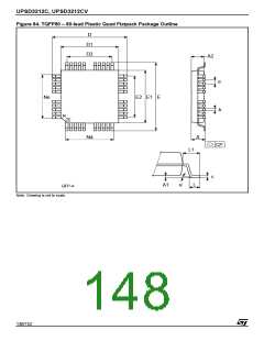
UPSD3212C, UPSD3212CV
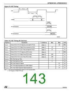
Table 117. ISC Timing (3V Devices)
Symbol
Parameter
Conditions
(Note 1)
(Note 1)
(Note 1)
(Note 2)
(Note 2)
(Note 2)
Min
Max
Unit
MHz
ns
t
Clock (TCK, PC1) Frequency (except for PLD)
Clock (TCK, PC1) High Time (except for PLD)
Clock (TCK, PC1) Low Time (except for PLD)
Clock (TCK, PC1) Frequency (PLD only)
Clock (TCK, PC1) High Time (PLD only)
12
ISCCF
t
t
t
t
40
40
ISCCH
ISCCL
ns
2
MHz
ns
ISCCFP
ISCCHP
240
t
t
t
t
t
t
Clock (TCK, PC1) Low Time (PLD only)
ISC Port Set Up Time
240
12
5
ns
ns
ns
ns
ns
ns
ISCCLP
ISCPSU
ISCPH
ISC Port Hold Up Time
ISC Port Clock to Output
30
30
30
ISCPCO
ISCPZV
ISCPVZ
ISC Port High-Impedance to Valid Output
ISC Port Valid Output to High-Impedance
Note: 1. For non-PLD Programming, Erase or in ISC By-pass Mode.
2. For Program or Erase PLD only.
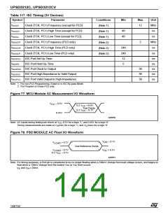
Figure 77. MCU Module AC Measurement I/O Waveform
V
– 0.5V
0.45V
CC
0.2 V
0.2 V
+ 0.9V
CC
Test Points
– 0.1V
CC
AI06650
Note: AC inputs during testing are driven at V –0.5V for a logic '1,' and 0.45V for a logic '0.'
CC
Timing measurements are made at V (min) for a logic '1,' and V (max) for a logic '0'
IH
IL
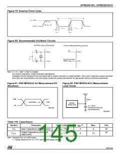
Figure 78. PSD MODULE AC Float I/O Waveform
V
V
– 0.1V
OH
OL
V
V
+ 0.1V
LOAD
Test Reference Points
– 0.1V
– 0.1V
+ 0.1V
LOAD
CC
0.2 V
AI06651
Note: For timing purposes, a Port pin is considered to be no longer floating when a 100mV change from load voltage occurs, and begins to
float when a 100mV change from the loaded V or V level occurs
OH
OL
I
and I ≥ 20mA
OH
OL
144/152

 STMICROELECTRONICS [ ST ]