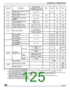
UPSD3212C, UPSD3212CV
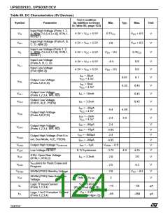
Test Condition
Symbol
Parameter
(in addition to those
Min.
Typ.
Max.
Unit
in Table 86, page 122)
SRAM (PSD) Standby Current
I
V
= 0V
0.5
1
µA
µA
µA
µA
STBY
CC
(V
input)
STBY
SRAM (PSD) Idle Current
(V input)
I
V
> V
–0.1
–10
–20
0.1
–55
–50
IDLE
CC STBY
STBY
Reset Pin Pull-up Current
(RESET)
I
V
= V
IN SS
RST
XTAL1 = V
XTAL2 = V
XTAL Feedback Resistor
Current (XTAL1)
CC
I
FR
SS
I
V
< V < V
SS IN CC
Input Leakage Current
Output Leakage Current
–1
1
µA
µA
LI
I
0.45 < V
< V
OUT CC
–10
10
LO
V
= 5.5V
CC
250
µA
LVD logic disabled
(1)
Power-down Mode
I
PD
LVD logic enabled
380
30
10
38
20
62
30
µA
mA
mA
mA
mA
mA
mA
Active (12MHz)
Idle (12MHz)
Active (24MHz)
Idle (24MHz)
Active (40MHz)
Idle (40MHz)
20
8
V
CC
V
CC
V
CC
= 5V
= 5V
= 5V
30
15
40
20
(2,3,5)
I
CC_CPU
PLD_TURBO = Off,
(5)
0
µA/PT
µA/PT
mA
(4)
f = 0MHz
PLD Only
PLD_TURBO = On,
f = 0MHz
400
15
700
30
I
CC_PSD
Operating
Supply Current
Flash
(5)
During Flash memory
WRITE/Erase Only
(DC)
memory
Read only, f = 0MHz
f = 0MHz
0
0
0
0
mA
mA
SRAM
PLD AC Base
Note 4
mA/
MHz
I
CC_PSD
(5)
Flash memory AC Adder
SRAM AC Adder
2.5
1.5
3.5
3.0
(AC)
mA/
MHz
Note: 1. I (Power-down Mode) is measured with:
PD
XTAL1=V ; XTAL2=not connected; RESET=V ; Port 0 =V ; all other pins are disconnected. PLD not in Turbo Mode.
SS
CC
CC
2. I
(active mode) is measured with:
CC_CPU
XTAL1 driven with t
, t
= 5ns, V = V +0.5V, V = Vcc – 0.5V, XTAL2 = not connected; RESET=V ; Port 0=V ; all
CLCH CHCL IL SS IH SS CC
other pins are disconnected. I would be slightly higher if a crystal oscillator is used (approximately 1mA).
CC
3. I
(Idle Mode) is measured with:
CC_CPU
XTAL1 driven with t
, t
= 5ns, V = V +0.5V, V = V – 0.5V, XTAL2 = not connected; Port 0 = V
;
CC
CLCH CHCL
IL
SS
IH
CC
RESET=V ; all other pins are disconnected.
CC
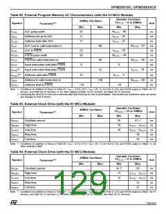
4. See Figure 62 for the PLD current calculation.
5. I/O current = 0 mA, all I/O pins are disconnected.
125/152

 STMICROELECTRONICS [ ST ]