UPSD3212C, UPSD3212CV
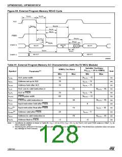
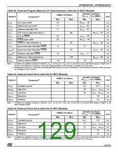
Table 92. External Program Memory AC Characteristics (with the 3V MCU Module)
Variable Oscillator
24MHz Oscillator
1/t
= 8 to 24MHz
(1)
CLCL
Symbol
Unit
Parameter
Min
43
Max
Min
– 40
CLCL
Max
t
2t
t
ALE pulse width
ns
ns
ns
ns
ns
ns
ns
ns
ns
LHLL
AVLL
LLAX
LLIV
t
t
t
t
t
t
t
– 25
Address set up to ALE
Address hold after ALE
17
CLCL
t
– 25
17
CLCL
4t
– 87
ALE Low to valid instruction in
ALE to PSEN
80
CLCL
t
– 20
– 30
22
95
LLPL
PLPH
PLIV
PXIX
CLCL
3t
PSEN pulse width
CLCL
3t
t
– 65
– 10
PSEN to valid instruction in
Input instruction hold after PSEN
Input instruction float after PSEN
60
32
CLCL
0
0
(2)
t
CLCL
PXIZ
(2)
t
– 5
Address valid after PSEN
Address to valid instruction in
Address float to PSEN
37
ns
ns
ns
t
t
t
CLCL
PXAV
5t
CLCL
– 60
148
AVIV
–10
–10
AZPL
Note: 1. Conditions (in addition to those in Table 87, V = 3.0 to 3.6V): V = 0V; C for Port 0, ALE and PSEN output is 100pF, for 5V
CC
SS
L
devices, and 50pF for 3V devices; C for other outputs is 80pF, for 5V devices, and 50pF for 3V devices)
L
2. Interfacing the uPSD321X Devices to devices with float times up to 35ns is permissible. This limited bus contention does not cause
any damage to Port 0 drivers.
Table 93. External Clock Drive (with the 5V MCU Module)
Variable Oscillator
40MHz Oscillator
1/t
= 24 to 40MHz
Max
(1)
CLCL
Symbol
Unit
Parameter
Min
Max
Min
25
t
Oscillator period
41.7
ns
ns
ns
ns
ns
RLRH
WLWH
LLAX2
RHDX
RHDX
t
t
t
t
t
t
– t
– t
10
10
High time
Low time
Rise time
Fall time
10
CLCL
CLCX
10
CLCL
CLCX
Note: 1. Conditions (in addition to those in Table 86, V = 4.5 to 5.5V): V = 0V; C for Port 0, ALE and PSEN output is 100pF; C for
CC
SS
L
L
other outputs is 80pF
Table 94. External Clock Drive (with the 3V MCU Module)
Variable Oscillator
24MHz Oscillator
1/t
= 8 to 24MHz
(1)
CLCL
Symbol
Unit
Parameter
Min
Max
Min
Max
t
Oscillator period
41.7
12
125
ns
ns
ns
ns
ns
RLRH
WLWH
LLAX2
RHDX
RHDX
t
t
t
t
t
t
– t
– t
12
12
High time
Low time
Rise time
Fall time
CLCL
CLCX
12
CLCL
CLCX
Note: 1. Conditions (in addition to those in Table 87, V = 3.0 to 3.6V): V = 0V; C for Port 0, ALE and PSEN output is 100pF, for 5V
CC
SS
L
devices, and 50pF for 3V devices; C for other outputs is 80pF, for 5V devices, and 50pF for 3V devices)
L
129/152

 STMICROELECTRONICS [ ST ]