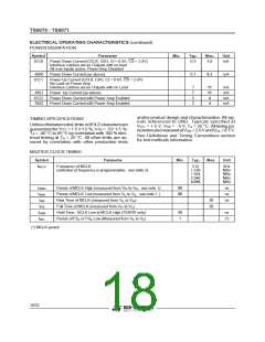
TS5070 - TS5071
foreany otherconnectionsaremadeshouldalways
be followed.Inapplicationswherethe printedcircuit
card may be pluggedinto a hot socket with power
and clocks already present, an extra long ground
pinontheconnectorshouldbe usedandaSchottky
diode connected between VSS and GND. To mini-
mize noise sourcesall groundconnectionsto each
device should meet at a common point as close as
possible to the GND pin in order to preventthe in-
teractionof groundreturn currents flowing through
a common bus impedance. Power supply decou-
plingcapacitorsof0.1µF shouldbe connectedfrom
this common device ground point to VCC and VSS
ascloseto thedevicepinsaspossible.VCC andVSS
should also be decoupledwith low effective series
resis-tancecapacitorsofatleast10 µF locatednear
the card edge connector.
APPLICATION INFORMATION
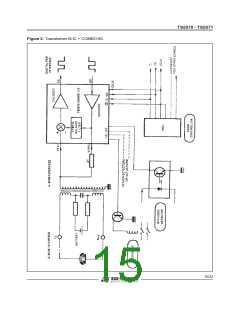
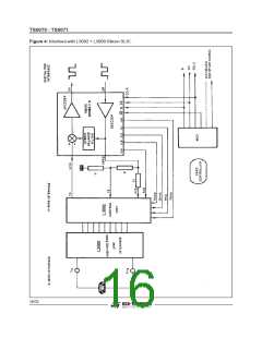
Figure 2 shows a typical applicationof the TS5070
together with a transformerSLIC.
The design of the transformer is greatly simplified
due to theon-chiphybridbalancecancellationfilter.
Only one singlesecondarywindingis required(see
application note AN.091 - Designing a subscriber
line card module using the TS5070/COMBO IIG).
Figures 3 and 4 show an arrangement with SGS-
Thomson monolithic SLICS.
POWER SUPPLIES
While the pins of theTS5070and TS5071/COMBO
IIG devices are well protected against electrical
misuse, it is recommended that the standard
CMOS practice of applying GND to the device be-
14/32

 STMICROELECTRONICS [ ST ]