STM32F405xx, STM32F407xx
Electrical characteristics
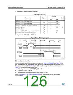
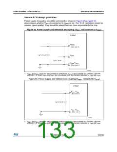
CAN (controller area network) interface
Refer to Section 5.3.16: I/O port characteristics for more details on the input/output alternate
function characteristics (CANTX and CANRX).
5.3.20
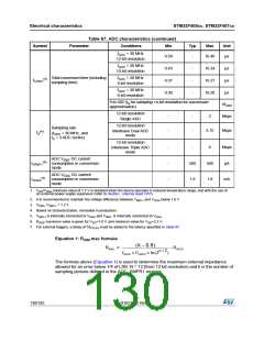
12-bit ADC characteristics
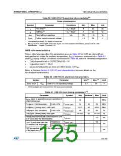
Unless otherwise specified, the parameters given in Table 67 are derived from tests
performed under the ambient temperature, f
frequency and V
supply voltage
PCLK2
DDA
conditions summarized in Table 14.
Table 67. ADC characteristics
Conditions
Symbol
Parameter
Power supply
Min
Typ
Max
Unit
VDDA
1.8(1)
-
-
3.6
V
V
VREF+ Positive reference voltage
1.8(1)(2)(3)
VDDA
VDDA = 1.8(1)(3) to
2.4 V
0.6
0.6
-
15
18
36
MHz
MHz
kHz
fADC
ADC clock frequency
VDDA = 2.4 to 3.6 V(3)
30
-
fADC = 30 MHz,
12-bit resolution
1764
17
(4)
fTRIG
External trigger frequency
Conversion voltage range(5)
-
-
1/fADC
V
0 (VSSA or VREF-
tied to ground)
VAIN
-
VREF+
See Equation 1 for
(4)
RAIN
External input impedance
Sampling switch resistance
-
-
-
-
-
50
6
κΩ
κΩ
pF
details
(4)(6)
RADC
Internal sample and hold
capacitor
(4)
CADC
4
-
fADC = 30 MHz
fADC = 30 MHz
-
-
-
0.100
3(7)
0.067
2(7)
16
µs
1/fADC
µs
Injection trigger conversion
latency
(4)
tlat
-
-
-
Regular trigger conversion
latency
(4)
tlatr
-
-
1/fADC
µs
f
ADC = 30 MHz
0.100
-
(4)
tS
Sampling time
Power-up time
3
-
-
480
3
1/fADC
µs
(4)
tSTAB
2
DocID022152 Rev 4
129/185

 STMICROELECTRONICS [ ST ]