STM32F405xx, STM32F407xx
Electrical characteristics
a
(1)
Table 68. ADC accuracy at f
= 30 MHz
ADC
Symbol
Parameter
Test conditions
Typ
Max(2)
Unit
ET
EO
EG
ED
EL
Total unadjusted error
Offset error
±2
±5
±2.5
±3
±1.5
±1.5
±1
f
PCLK2 = 60 MHz,
Gain error
fADC = 30 MHz, RAIN < 10 kΩ,
LSB
VDDA = 1.8(3) to 3.6 V
Differential linearity error
Integral linearity error
±2
±1.5
±3
1. Better performance could be achieved in restricted VDD, frequency and temperature ranges.
2. Based on characterization, not tested in production.
3. VDD/VDDA minimum value of 1.7 V is obtained when the device operates in reduced temperature range,
and with the use of an external power supply supervisor (refer to Section : Internal reset OFF).
Note:
ADC accuracy vs. negative injection current: injecting a negative current on any analog
input pins should be avoided as this significantly reduces the accuracy of the conversion
being performed on another analog input. It is recommended to add a Schottky diode (pin to
ground) to analog pins which may potentially inject negative currents.
Any positive injection current within the limits specified for I
Section 5.3.16 does not affect the ADC accuracy.
and ΣI
in
INJ(PIN)
INJ(PIN)
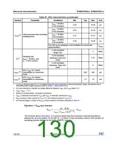
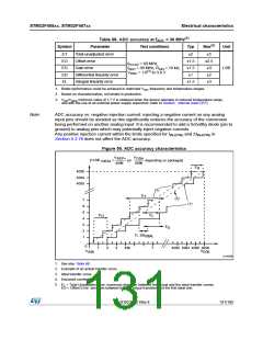
Figure 50. ADC accuracy characteristics
V
V
DDA
4096
REF+
[1LSB
=
(or
depending on package)]
IDEAL
4096
E
G
4095
4094
4093
(2)
E
T
(3)
7
6
5
4
3
2
1
(1)
E
E
O
L
E
D
1L SB
IDEAL
7
0
V
1
2
3
456
4093 4094 4095 4096
V
DDA
SSA
ai14395c
1. See also Table 68.
2. Example of an actual transfer curve.
3. Ideal transfer curve.
4. End point correlation line.
5. ET = Total Unadjusted Error: maximum deviation between the actual and the ideal transfer curves.
EO = Offset Error: deviation between the first actual transition and the first ideal one.
DocID022152 Rev 4
131/185

 STMICROELECTRONICS [ ST ]