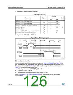
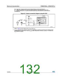
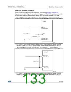
Electrical characteristics
STM32F405xx, STM32F407xx
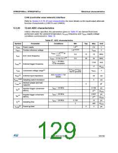
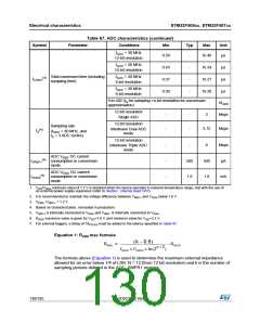
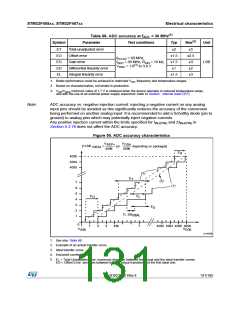
Table 67. ADC characteristics (continued)
Symbol
Parameter
Conditions
Min
Typ
Max
Unit
fADC = 30 MHz
12-bit resolution
0.50
-
16.40
µs
fADC = 30 MHz
10-bit resolution
0.43
0.37
0.30
-
-
-
16.34
16.27
16.20
µs
µs
Total conversion time (including
sampling time)
fADC = 30 MHz
8-bit resolution
(4)
tCONV
fADC = 30 MHz
6-bit resolution
µs
9 to 492 (tS for sampling +n-bit resolution for successive
approximation)
1/fADC
Msps
12-bit resolution
-
-
-
-
2
Single ADC
12-bit resolution
Sampling rate
3.75
Msps
Interleave Dual ADC
mode
(4)
fS
(fADC = 30 MHz, and
tS = 3 ADC cycles)
12-bit resolution
-
-
-
-
6
Msps
µA
Interleave Triple ADC
mode
ADC VREF DC current
consumption in conversion
mode
(4)
IVREF+
300
1.6
500
1.8
ADC VDDA DC current
consumption in conversion
mode
(4)
IVDDA
mA
1. VDD/VDDA minimum value of 1.7 V is obtained when the device operates in reduced temperature range, and with the use of
an external power supply supervisor (refer to Section : Internal reset OFF).
2. It is recommended to maintain the voltage difference between VREF+ and VDDA below 1.8 V.
3. VDDA -VREF+ < 1.2 V.
4. Based on characterization, not tested in production.
5. VREF+ is internally connected to VDDA and VREF- is internally connected to VSSA
.
6. RADC maximum value is given for VDD=1.8 V, and minimum value for VDD=3.3 V.
7. For external triggers, a delay of 1/fPCLK2 must be added to the latency specified in Table 67.
Equation 1: R
max formula
AIN
(k – 0.5)
RAIN = -------------------------------------------------------------- – RADC
fADC × CADC × ln(2N + 2
)
The formula above (Equation 1) is used to determine the maximum external impedance
allowed for an error below 1/4 of LSB. N = 12 (from 12-bit resolution) and k is the number of
sampling periods defined in the ADC_SMPR1 register.
130/185
DocID022152 Rev 4

 STMICROELECTRONICS [ ST ]