Electrical characteristics
STM32F405xx, STM32F407xx
1. Guaranteed by design, not tested in production.
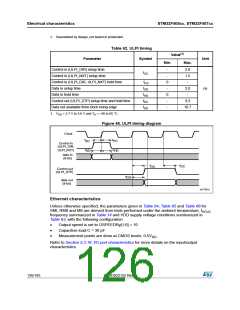
Table 62. ULPI timing
Value(1)
Parameter
Symbol
Unit
Min.
Max.
Control in (ULPI_DIR) setup time
Control in (ULPI_NXT) setup time
Control in (ULPI_DIR, ULPI_NXT) hold time
Data in setup time
-
-
2.0
1.5
-
tSC
tHC
tSD
tHD
tDC
tDD
0
-
2.0
-
ns
Data in hold time
0
-
Control out (ULPI_STP) setup time and hold time
Data out available from clock rising edge
1. VDD = 2.7 V to 3.6 V and TA = –40 to 85 °C.
9.2
10.7
-
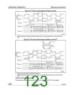
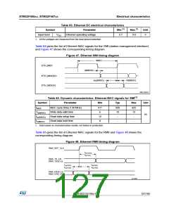
Figure 46. ULPI timing diagram
Clock
t
t
HC
SC
Control In
(ULPI_DIR,
ULPI_NXT)
t
t
HD
SD
data In
(8-bit)
t
t
DC
DC
Control out
(ULPI_STP)
t
DD
data out
(8-bit)
ai17361c
Ethernet characteristics
Unless otherwise specified, the parameters given in Table 64, Table 65 and Table 66 for
SMI, RMII and MII are derived from tests performed under the ambient temperature, f
HCLK
frequency summarized in Table 14 and VDD supply voltage conditions summarized in
Table 63, with the following configuration:
•
•
•
Output speed is set to OSPEEDRy[1:0] = 10
Capacitive load C = 30 pF
Measurement points are done at CMOS levels: 0.5V
.
DD
Refer to Section 5.3.16: I/O port characteristics for more details on the input/output
characteristics.
126/185
DocID022152 Rev 4

 STMICROELECTRONICS [ ST ]