STM32F405xx, STM32F407xx
Electrical characteristics
(1)
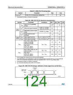
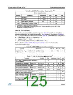
Table 59. USB OTG FS electrical characteristics
Driver characteristics
Conditions
Symbol
Parameter
Rise time(2)
Fall time(2)
Rise/ fall time matching
Output signal crossover voltage
Min
Max
Unit
tr
tf
CL = 50 pF
CL = 50 pF
tr/tf
4
4
20
20
ns
ns
%
V
trfm
VCRS
90
1.3
110
2.0
1. Guaranteed by design, not tested in production.
Measured from 10% to 90% of the data signal. For more detailed informations, please refer to USB
Specification - Chapter 7 (version 2.0).
2.
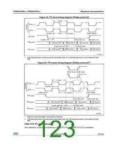
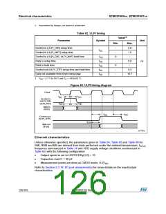
USB HS characteristics
Unless otherwise specified, the parameters given in Table 62 for ULPI are derived from
tests performed under the ambient temperature, f frequency summarized in Table 61
HCLK
and V supply voltage conditions summarized in Table 60, with the following configuration:
DD
•
•
•
Output speed is set to OSPEEDRy[1:0] = 10
Capacitive load C = 30 pF
Measurement points are done at CMOS levels: 0.5V
.
DD
Refer to Section Section 5.3.16: I/O port characteristics for more details on the
input/outputcharacteristics.
Table 60. USB HS DC electrical characteristics
Symbol
Input level
Parameter
Min.(1)
Max.(1)
Unit
VDD
USB OTG HS operating voltage
2.7
3.6
V
1. All the voltages are measured from the local ground potential.
(1)
Table 61. USB HS clock timing parameters
Parameter
Symbol
Min
Nominal
Max
Unit
f
HCLK value to guarantee proper operation of
30
MHz
USB HS interface
Frequency (first transition)
8-bit ±10%
FSTART_8BIT
FSTEADY
DSTART_8BIT
DSTEADY
54
59.97
40
60
60
50
50
66
60.03
60
MHz
MHz
%
Frequency (steady state) ±500 ppm
Duty cycle (first transition)
8-bit ±10%
Duty cycle (steady state) ±500 ppm
49.975
50.025
%
Time to reach the steady state frequency and
duty cycle after the first transition
TSTEADY
-
-
1.4
ms
ms
µs
Peripheral
TSTART_DEV
-
-
-
-
5.6
-
Clock startup time after the
de-assertion of SuspendM
Host
TSTART_HOST
PHY preparation time after the first transition
of the input clock
TPREP
-
-
-
DocID022152 Rev 4
125/185

 STMICROELECTRONICS [ ST ]