STM32F405xx, STM32F407xx
Electrical characteristics
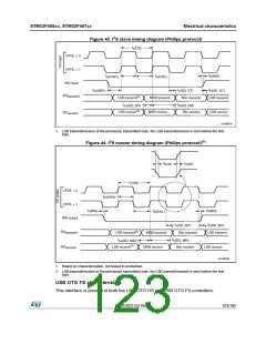
(1)
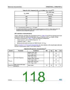
Table 55. SPI dynamic characteristics (continued)
Symbol
Parameter
Conditions
Min
TPCLK-0.5 TPCLK TPCLK+0.5
PCLK-2 TPCLK TPCLK+2
Typ
Max
Unit
Master mode, SPI presc = 2,
2.7V < VDD < 3.6V
tw(SCKH)
SCK high and low time
Master mode, SPI presc = 2,
1.7V < VDD < 3.6V
tw(SCKL)
T
tsu(NSS)
th(NSS)
tsu(MI)
tsu(SI)
th(MI)
NSS setup time
NSS hold time
Slave mode, SPI presc = 2
Slave mode, SPI presc = 2
Master mode
4 x TPCLK
-
-
2 x TPCLK
6.5
2.5
2.5
4
-
-
-
-
-
-
Data input setup time
Slave mode
-
Master mode
-
Data input hold time
th(SI)
Slave mode
-
(2)
ta(SO)
Data output access time
Slave mode, SPI presc = 2
0
4 x TPCLK
Slave mode, SPI1,
2.7V < VDD < 3.6V
0
0
-
-
-
7.5
16.5
13
(3)
tdis(SO)
Data output disable time
Slave mode, SPI1/2/3
1.7V < VDD < 3.6V
ns
Slave mode (after enable edge),
SPI1, 2.7V < VDD < 3.6V
11
12
15.5
18
-
Slave mode (after enable edge),
SPI2/3, 2.7V < VDD < 3.6V
-
16.5
19
tv(SO)
th(SO)
Data output valid/hold time
Slave mode (after enable edge),
SPI1, 1.7V < VDD < 3.6V
-
Slave mode (after enable edge),
SPI2/3, 1.7V < VDD < 3.6V
-
20.5
2.5
4.5
-
Master mode (after enable edge),
SPI1 , 2.7V < VDD < 3.6V
-
tv(MO)
Data output valid time
Data output hold time
Master mode (after enable edge),
SPI1/2/3 , 1.7V < VDD < 3.6V
-
-
th(MO)
Master mode (after enable edge)
0
-
1. Data based on characterization results, not tested in production.
2. Min time is for the minimum time to drive the output and the max time is for the maximum time to validate the data.
3. Min time is for the minimum time to invalidate the output and the max time is for the maximum time to put the data in Hi-Z.
DocID022152 Rev 4
119/185

 STMICROELECTRONICS [ ST ]