Electrical characteristics
STM32F405xx, STM32F407xx
Max vs.
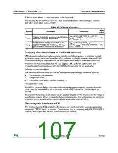
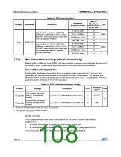
Table 43. EMI characteristics
Monitored
frequency band
[fHSE/fCPU
]
Symbol
Parameter
Conditions
Unit
25/168 MHz
0.1 to 30 MHz
30 to 130 MHz
130 MHz to 1GHz
SAE EMI Level
0.1 to 30 MHz
32
25
29
4
VDD = 3.3 V, TA = 25 °C, LQFP176
package, conforming to SAE J1752/3
EEMBC, code running from Flash with
ART accelerator enabled
dBµV
-
dBµV
-
SEMI
Peak level
19
16
18
3.5
VDD = 3.3 V, TA = 25 °C, LQFP176
package, conforming to SAE J1752/3
EEMBC, code running from Flash with
ART accelerator and PLL spread
spectrum enabled
30 to 130 MHz
130 MHz to 1GHz
SAE EMI level
5.3.14
Absolute maximum ratings (electrical sensitivity)
Based on three different tests (ESD, LU) using specific measurement methods, the device is
stressed in order to determine its performance in terms of electrical sensitivity.
Electrostatic discharge (ESD)
Electrostatic discharges (a positive then a negative pulse separated by 1 second) are
applied to the pins of each sample according to each pin combination. The sample size
depends on the number of supply pins in the device (3 parts × (n+1) supply pins). This test
conforms to the JESD22-A114/C101 standard.
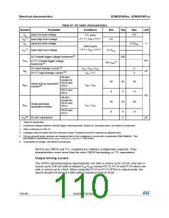
Table 44. ESD absolute maximum ratings
Maximum
Symbol
Ratings
Conditions
Class
Unit
value(1)
Electrostatic discharge
VESD(HBM) voltage (human body
model)
TA = +25 °C conforming to JESD22-A114
2
2000(2)
V
Electrostatic discharge
VESD(CDM) voltage (charge device
model)
TA = +25 °C conforming to JESD22-C101
II
500
1. Based on characterization results, not tested in production.
2. On VBAT pin, VESD(HBM) is limited to 1000 V.
Static latchup
Two complementary static tests are required on six parts to assess the latchup
performance:
•
•
A supply overvoltage is applied to each power supply pin
A current injection is applied to each input, output and configurable I/O pin
These tests are compliant with EIA/JESD 78A IC latchup standard.
108/185
DocID022152 Rev 4

 STMICROELECTRONICS [ ST ]