Electrical characteristics
STM32F405xx, STM32F407xx
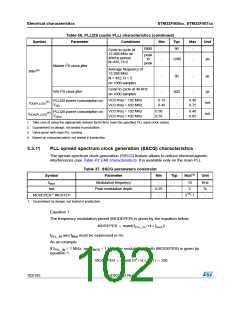
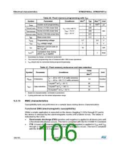
Table 40. Flash memory programming with V
PP
Symbol
Parameter
Conditions
Min(1)
Typ
Max(1) Unit
tprog
Double word programming
-
-
16
230
490
875
6.9
-
100(2)
µs
tERASE16KB Sector (16 KB) erase time
tERASE64KB Sector (64 KB) erase time
tERASE128KB Sector (128 KB) erase time
-
-
TA = 0 to +40 °C
VDD = 3.3 V
-
ms
VPP = 8.5 V
-
-
tME
Vprog
VPP
Mass erase time
-
-
s
V
V
Programming voltage
VPP voltage range
2.7
7
3.6
9
-
Minimum current sunk on
the VPP pin
IPP
10
-
-
-
-
mA
Cumulative time during
which VPP is applied
(3)
tVPP
1
hour
1. Guaranteed by design, not tested in production.
2. The maximum programming time is measured after 100K erase operations.
3. VPP should only be connected during programming/erasing.
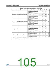
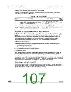
Table 41. Flash memory endurance and data retention
Value
Symbol
Parameter
Conditions
Unit
Min(1)
TA = –40 to +85 °C (6 suffix versions)
TA = –40 to +105 °C (7 suffix versions)
NEND Endurance
kcycles
Years
10
1 kcycle(2) at TA = 85 °C
30
10
20
tRET
Data retention 1 kcycle(2) at TA = 105 °C
10 kcycles(2) at TA = 55 °C
1. Based on characterization, not tested in production.
2. Cycling performed over the whole temperature range.
5.3.13
EMC characteristics
Susceptibility tests are performed on a sample basis during device characterization.
Functional EMS (electromagnetic susceptibility)
While a simple application is executed on the device (toggling 2 LEDs through I/O ports).
the device is stressed by two electromagnetic events until a failure occurs. The failure is
indicated by the LEDs:
•
Electrostatic discharge (ESD) (positive and negative) is applied to all device pins until
a functional disturbance occurs. This test is compliant with the IEC 61000-4-2 standard.
•
FTB: A burst of fast transient voltage (positive and negative) is applied to V and V
through a 100 pF capacitor, until a functional disturbance occurs. This test is compliant
with the IEC 61000-4-4 standard.
DD
SS
106/185
DocID022152 Rev 4

 STMICROELECTRONICS [ ST ]