STM32F302xx/STM32F303xx
Electrical characteristics
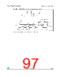
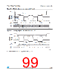
Figure 26. SPI timing diagram - slave mode and CPHA = 0
NSS input
t
c(SCK)
t
t
h(NSS)
SU(NSS)
CPHA=0
CPOL=0
t
t
w(SCKH)
w(SCKL)
CPHA=0
CPOL=1
t
t
t
t
t
t
dis(SO)
r(SCK)
f(SCK)
v(SO)
a(SO)
h(SO)
MISO
OUT PUT
MSB O UT
BI T6 OUT
BIT1 IN
LSB OUT
t
su(SI)
MOSI
M SB IN
LSB IN
INPUT
t
h(SI)
ai14134c
(1)
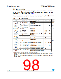
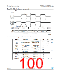
Figure 27. SPI timing diagram - slave mode and CPHA = 1
NSS input
t
t
t
SU(NSS)
t
c(SCK)
h(NSS)
CPHA=1
CPOL=0
w(SCKH)
CPHA=1
CPOL=1
t
w(SCKL)
t
t
r(SCK)
f(SCK)
t
t
t
v(SO)
h(SO)
dis(SO)
t
a(SO)
MISO
OUT PUT
MSB O UT
BI T6 OUT
LSB OUT
t
t
su(SI)
h(SI)
MOSI
M SB IN
BIT1 IN
LSB IN
INPUT
ai14135
1. Measurement points are done at 0.5VDD and with external CL = 30 pF.
Doc ID 023353 Rev 5
99/133

 STMICROELECTRONICS [ ST ]