STM32F302xx/STM32F303xx
Electrical characteristics
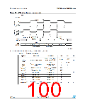
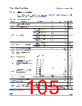
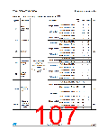
Table 64. USB DC electrical characteristics
Symbol
Parameter
Conditions
Min.(1)
Max.(1) Unit
Input levels
VDD
USB operating voltage(2)
3.0(3)
0.2
3.6
-
V
V
(4)
VDI
Differential input sensitivity
Differential common mode range
Single ended receiver threshold
I(USB_DP, USB_DM)
Includes VDI range
(4)
VCM
0.8
2.5
2.0
(4)
VSE
Output levels
1.3
VOL
VOH
Static output level low
Static output level high
RL of 1.5 kΩ to 3.6 V(5)
-
0.3
3.6
V
(5)
RL of 15 kΩ to VSS
2.8
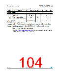
1. All the voltages are measured from the local ground potential.
2. To be compliant with the USB 2.0 full-speed electrical specification, the USB_DP (D+) pin should be pulled
up with a 1.5 kΩ resistor to a 3.0-to-3.6 V voltage range.
3. The STM32F3xxx USB functionality is ensured down to 2.7 V but not the full USB electrical characteristics
which are degraded in the 2.7-to-3.0 V VDD voltage range.
4. Guaranteed by design, not tested in production.
RL is the load connected on the USB drivers
5.
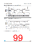
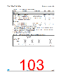
Figure 31. USB timings: definition of data signal rise and fall time
Crossover
points
Differential
Data Lines
V
CR S
V
SS
t
t
r
f
ai14137
Doc ID 023353 Rev 5
103/133

 STMICROELECTRONICS [ ST ]