Electrical characteristics
STM32F302xx/STM32F303xx
(1)
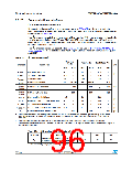
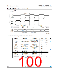
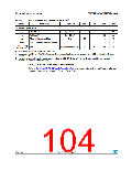
Figure 28. SPI timing diagram - master mode
(IGH
.33 INPUT
T
Cꢐ3#+ꢑ
#0(!ꢓꢄ
#0/,ꢓꢄ
#0(!ꢓꢄ
#0/,ꢓꢃ
#0(!ꢓꢃ
#0/,ꢓꢄ
#0(!ꢓꢃ
#0/,ꢓꢃ
T
T
T
T
Wꢐ3#+(ꢑ
Wꢐ3#+,ꢑ
Rꢐ3#+ꢑ
Fꢐ3#+ꢑ
T
SUꢐ-)ꢑ
-)3/
).054
-3").
")4ꢂ ).
,3" ).
T
Hꢐ-)ꢑ
-/3)
- 3" /54
")4ꢃ /54
,3" /54
/54054
T
T
Vꢐ-/ꢑ
Hꢐ-/ꢑ
AIꢃꢀꢃꢈꢂ6ꢉ
1. Measurement points are done at 0.5VDD and with external CL = 30 pF.
2
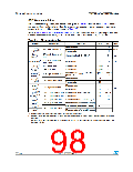
Table 62. I S characteristics
Symbol
Parameter
Conditions
Min
Max
Unit
Master data: 16 bits,
audio freq=48 kHz
1.496
1.503
12.288
8
fCK
1/tc(CK)
I2S clock frequency
MHz
(1)
Slave
0
-
tr(CK)
I2S clock rise and fall
time
Capacitive load
CL = 30 pF
(1)
tf(CK)
tw(CKH)
I2S clock high time
I2S clock low time
Master fPCLK= 36 MHz,
audio frequency =
48 kHz
331
332
-
-
(1)
(1)
tw(CKL)
ns
%
(1)
(1)
(1)
(1)
tv(WS)
th(WS)
tsu(WS)
th(WS)
WS valid time
WS hold time
WS setup time
WS hold time
Master mode
Master mode
Slave mode
Slave mode
4
4
4
0
-
-
-
-
I2S slave input clock
duty cycle
Duty Cycle(1)
Slave mode
30
70
100/133
Doc ID 023353 Rev 5

 STMICROELECTRONICS [ ST ]