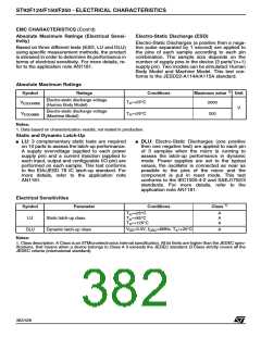
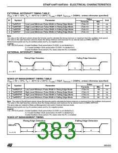
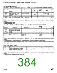
ST92F124/F150/F250 - ELECTRICAL CHARACTERISTICS
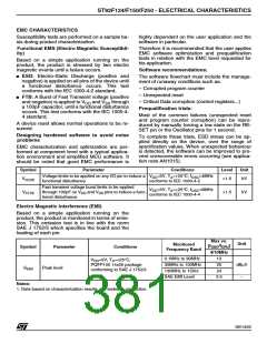
EMC CHARACTERISTICS
Susceptibility tests are performed on a sample ba-
sis during product characterization.
highly dependent on the user application and the
software in particular.
Functional EMS (Electro Magnetic Susceptibil-
ity)
Therefore it is recommended that the user applies
EMC software optimization and prequalification
tests in relation with the EMC level requested for
his application.
Based on a simple application running on the
product, the product is stressed by two electro
magnetic events until a failure occurs.
Software recommendations:
■ ESD: Electro-Static Discharge (positive and
negative) is applied on all pins of the device until
a functional disturbance occurs. This test
conforms with the IEC 1000-4-2 standard.
The software flowchart must include the manage-
ment of runaway conditions such as:
– Corrupted program counter
– Unexpected reset
■ FTB: A Burst of Fast Transient voltage (positive
– Critical Data corruption (control registers...)
Prequalification trials:
and negative) is applied to V and V through
DD
SS
a 100pF capacitor, until a functional disturbance
occurs. This test conforms with the IEC 1000-4-
4 standard.
Most of the common failures (unexpected reset
and program counter corruption) can be repro-
duced by manually forcing a low state on the RE-
SET pin or the Oscillator pins for 1 second.
A device reset allows normal operations to be re-
sumed.
Designing hardened software to avoid noise
problems
To complete these trials, ESD stress can be ap-
plied directly on the device, over the range of
specification values. When unexpected behaviour
is detected, the software can be improved to pre-
vent unrecoverable errors occurring (see applica-
tion note AN1015).
EMC characterization and optimization are per-
formed at component level with a typical applica-
tion environment and simplified MCU software. It
should be noted that good EMC performance is
Symbol
Parameter
Conditions
=5V, T =+25°C, f
conforms to IEC 1000-4-2
Level
Unit
Voltage limits to be applied on any I/O pin to induce a
functional disturbance
V
=4MHz
OSC
DD
A
V
>1.5
kV
FESD
Fast transient voltage burst limits to be applied
V
=5V, T =+25°C, f =8MHz
DD
A
OSC
V
through 100pF on V and V pins to induce a func-
>1.5
kV
FFTB
DD
DD
conforms to IEC 1000-4-4
tional disturbance
Electro Magnetic Interference (EMI)
Based on a simple application running on the
product, the product is monitored in terms of emis-
sion. This emission test is in line with the norm
SAE J 1752/3 which specifies the board and the
loading of each pin.
Max vs.
[f /f ]
OSC CPU
Unit
Monitored
Frequency Band
Symbol
Parameter
Conditions
4/10MHz
13
0.1MHz to 30MHz
30MHz to 130MHz
130MHz to 1GHz
SAE EMI Level
V
=5V, T =+25°C,
A
PQFP100 14x20 package
conforming to SAE J 1752/3
DD
25
dBµV
S
Peak level
EMI
24
3.5
-
Notes:
1. Data based on characterization results, not tested in production.
381/426
1

 STMICROELECTRONICS [ ST ]