ST92F124/F150/F250 - ELECTRICAL CHARACTERISTICS
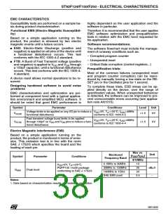
Value
Symbol
Parameter
Comment
Unit
Typ
Min
Max
(1)
Push Pull or
Open Drain mode,
I =8mA,
OL
Output Low Level
P4[7:6]-P6[5:4]
0.4
V
V
(3)
EMR1.BSZ bit = 1
V
OL
Push Pull or
Open Drain mode,
Output Low Level
All pins except OSCOUT
0.4
300
450
I
=2mA
OL
Weak Pull-up Current
Bidirectional
Weak Pull-up mode
= 0V
P2[7:4]-P2[1:0]-P3[7:0]
P4[7:5]-P4[3:1]-P5.3-P6[7:6]-P6[3:0]-
P7[7:0]-P8[7:0]-P9[7:0]
50
100
220
µA
µA
V
IN
I
WPU
Bidirectional
Weak Pull-up mode
Weak Pull-up Current
P6[5:4]-AS-DS-RW
100
V
= 0V
IN
Input or Tri-State mode,
0V < V < V
I
I/O Pin Input Leakage
– 1
– 1
1
1
µA
µA
LKIO
IN
DD
Input or Tri-State mode,
0V < V < V
I
I/O Pin Open Drain Input Leakage
LKIOD
IN
DD
V <V | I |< 400µA
ADC Conv.Input leakage current on ro-
bust pins
|
IN
SS, IN
6
1
µA
µA
on robust analog pin
|I
LKADC
ADC Conv.Input leakage current
V
SS≤V ≤V
IN
DD
P4[7:6]-P6[5:4]
EMR1.BSZ bit = 1
(4)
8
(3)
(3)
P4[7:6]-P6[5:4]
EMR1.BSZ bit = 0
(4)
I
Load current
2
mA
IO
All other pins except
OSCOUT
(4)
2
(5)
(4)
⎥I
⎥
Overload Current
Slew Rate Rise
Slew Rate Fall
5
mA
ns
OV
(6)
(6)
SR
20
20
30
30
R
SR
ns
F
Note:
(1) Unless otherwise stated, typical data are based on T = 25°C and V = 5V. They are only reported for design guide lines not tested in
A
DD
production.
(2) Value guaranteed by characterisation.
(3) For a description of the EMR1 Register - BSZ bit refer to the External Memory Interface Chapter.
(4) Value guaranteed by Design.
(5) Not tested in production, guaranteed by product characterisation. An overload condition occurs when the input voltage on any pin ex-
ceeds the specified voltage range.
(6) Indicative values extracted from design simulation, 20% to 80% on 50pF load, EMR1.BSZ bit =0.
377/426
1

 STMICROELECTRONICS [ ST ]