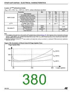
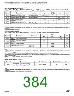
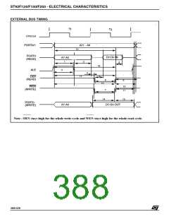
ST92F124/F150/F250 - ELECTRICAL CHARACTERISTICS
RCCU CHARACTERISTICS
(V = 5V ± 10%, T = –40°C to +125°C, C
= 50pF, f = 24MHz, unless otherwise specified)
DD
A
Load
INTCLK
Value
Symbol
Parameter
Comment
Unit
(1)
Min
Typ
Max
V
RESET Input High Level
RESET Input Low Level
Input Voltage Range
Input Threshold
Input Threshold
0.75 x V
– 0.3
– 1
V
V
IHRS
DD
V
0.25 x V
ILRS
DD
V
V
+ 0.3
DD
V
IRS
(2)
V
RESET Input Hysteresis
RESET Pin Input Leakage
1
V
HYRS
LKRS
I
0V < V < V
1
µA
IN
DD
Note:
(1) Unless otherwise stated, typical data are based on T = 25°C and V = 5V. They are only reported for design guide lines not tested in
A
DD
production.
(2) Value guaranteed by design.
RCCU TIMING TABLE
(V = 5V ± 10%, T = –40°C to +125°C, f
= 24 MHz, unless otherwise specified)
DD
A
INTCLK
Value
Symbol
Parameter
Comment
Unit
(1)
Min
Typ
Max
(2)
t
t
RESET Input Filtered Pulse
RESET Input Non Filtered
Pulse
50
ns
FRS
20
µs
(2)
NFR
(3)
t
RESET Phase duration
20400
T
T
RSPH
osc
osc
DIV2 = 0
DIV2 = 1
10200
20400
t
STOP Restart duration
STR
Note:
(1) Unless otherwise stated, typical data are based on T = 25°C and V = 5V. They are only reported for design guide lines not tested in
production.
A
DD
(2) To be valid, a RESET pulse must exceed t
. All reset glitches with a duration shorter than t
will be filtered
NFR
FRS
(3) Depending on the delay between rising edge of RESET pin and the first rising edge of CLOCK1, the value can differ from the typical value
for +/- 1 CLOCK1 cycle.
Legend: T
= Crystal Oscilllator Clock (CLOCK1) period.
osc
BOOTROM TIMING TABLE
(1)
Symbol
Parameter
Conditions
= 4MHz
Typ Value
Unit
BOOTROM Execution Duration
(see Figure 65 on page 136)
t
f
33
ms
(2)
BRE
OSC
Note:
(1) Unless otherwise stated, typical data are based on T = 25°C and V = 5V. They are only reported for design guide lines not tested in
A
DD
production
(2) Refer to AN1528 for more details on BOOTROM code.
384/426
1

 STMICROELECTRONICS [ ST ]