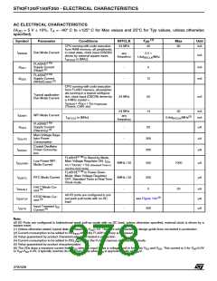
ST92F124/F150/F250 - ELECTRICAL CHARACTERISTICS
AC ELECTRICAL CHARACTERISTICS
(V
= 5 V ± 10%, T = –40° C to +125° C for Max values and 25°C for Typ values, unless otherwise
A
DD
specified)
(1)
Symbol
Parameter
Conditions
INTCLK
Typ
Max
Unit
CPU running with code execution
from RAM memory, all peripherals
in reset state, clock input (OSCIN)
driven by external square wave.
24 MHz
45
60
mA
I
Run Mode Current
2.5 +
DDRUN
any
frequency
mA
1.8xf
/MHz
INTCLK
f
in [MHz].
INTCLK
3 TM
FLASH/E
∆I
∆I
Supply Current
(Read)
-
-
2
mA
mA
DD1
DD2
(2)
3 TM
FLASH/E
Supply Current
12
(2)
(Write/Erase)
CPU running with code execution
from FLASH memory, all peripher-
als running in a typical configura-
tion, clock input (OSCIN) driven by
a 4-MHz crystal =
Typical application
Run Mode Current
24 MHz
24 MHz
50
14
mA
I
+ ∆I
+ I
DDRUN
DD1 DD Peripherals
(Timers, CAN, etc)
22
mA
mA
I
WFI Mode Current
DDWFI
any
frequency
(3)
f
in [MHz].
0.9xf
/MHz
INTCLK
INTCLK
3 TM
FLASH/E
∆I
Supply Current
(Stand-by)
-
-
20
µA
µA
µA
DD3
(4)
Main Voltage Regu-
lator Power
Consumption
I
300
200
DDLPR
Crystal Oscillator
Power Consump-
tion
I
DDOSC
3 TM
FLASH/E
in Stand-by Mode,
Low Power WFI
Mode Current
Main Voltage Regulator ON, I
DDL-
I
4MHz / 32
550
1000
µA
µA
DDLPWFI
+ I
+ I
DD (Standard Timer in
PR
DDOSC
real time clock mode)
3 TM
FLASH/E
in Power-Down
Mode, Main Voltage Regulator
OFF, Standard Timer in Real Time
Clock mode
I
RTC Mode Current
HALT Mode Cur-
4MHz / 32
-
250
5
DDRTC
I
25
µA
µA
µA
(5)
DDHALT
rent
All I/O ports are configured in out-
put push-pull mode with no DC
load
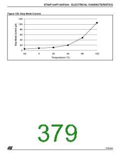
STOP Mode Cur-
(3)
I
see Figure 159
300
(3)
DDSTOP
rent
Input Transient I
DD
I
-
(6)
DDTR
Current
Note:
All I/O Ports are configured in bidirectional weak pull-up mode with no DC load, unless otherwise specified, external clock is driven by a
square wave.
(1) Unless otherwise stated, typical data are based on V = 5V. They are only reported for design guide lines not tested in production.
DD
(2) Current consumption to be added to IDD
when the FLASH memory is accessed.
RUN
(3) Value guaranteed by product characterization. Not tested in production.
(4) Current consumption to be added to IDD when the FLASH memory is in stand-by mode.
LPWFI
(5) Value guaranteed by product characterization.
(6) The I/Os draw a transient current from V when an input takes a voltage level in between V and V . This current is 0 for V <0.3V
DD
SS
DD
IN
or V >V -0.3V, it typically reaches its maximum value when V is approximatively at V /2.
IN
DD
IN
DD
378/426
1

 STMICROELECTRONICS [ ST ]