CONTROLLER AREA NETWORK (bxCAN)
CONTROLLER AREA NETWORK (Cont’d)
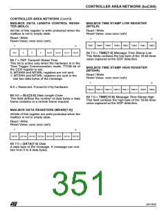
MAILBOX DATA LENGTH CONTROL REGIS-
TER (MDLC)
MAILBOX TIME STAMP LOW REGISTER
(MTSLR)
All bits of this register is write protected when the
mailbox is not in empty state.
Read / Write
Reset Value: xxxx xxxx (xxh)
Read / Write
Reset Value: xxxx xxxx (xxh)
7
0
TIME7 TIME6 TIME5 TIME4 TIME3 TIME2 TIME1 TIME0
7
0
TGT
0
0
0
DLC3
DLC2
DLC1
DLC0
Bit 7:0 = TIME[7:0] Message Time Stamp Low
This fields contains the low byte of the 16-bit timer
value captured at the SOF detection.
Bit 7 = TGT Transmit Global Time
This bit is active only when the hardware is in the
Time Trigger Communication mode, TTCM bit of
the CCR register is set.
0: MTSRH and MTSRL registers are not sent.
1: MTSRH and MTSRL registers are sent in the
last two data bytes of the message.
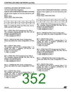
MAILBOX TIME STAMP HIGH REGISTER
(MTSHR)
Read / Write
Reset Value: xxxx xxxx (xxh)
7
0
6:4 = Reserved. Forced to 0 by hardware.
TIME15 TIME14 TIME13 TIME12 TIME11 TIME10 TIME9 TIME8
Bit 3:0 = DLC[3:0] Data Length Code
This field defines the number of data bytes a data
frame contains or a remote frame request.
Bit 7:0 = TIME[15:8] Message Time Stamp High
This field contains the high byte of the 16-bit timer
value captured at the SOF detection.
MAILBOX DATA REGISTERS (MDAR[7:0])
All bits of this register are write protected when the
mailbox is not in empty state.
Read / Write
Reset Value: xxxx xxxx (xxh)
7
0
DATA7 DATA6 DATA5 DATA4 DATA3 DATA2 DATA1 DATA0
Bit 7:0 = DATA[7:0] Data
A data byte of the message. A message can con-
tain from 0 to 8 data bytes.
351/426
9

 STMICROELECTRONICS [ ST ]