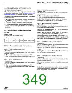
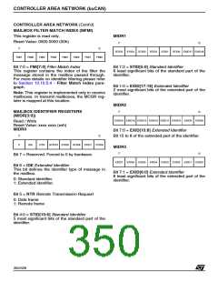
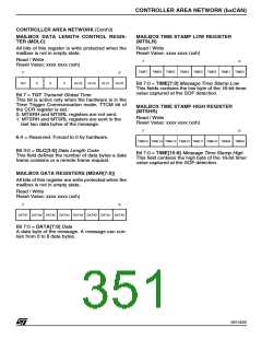
CONTROLLER AREA NETWORK (bxCAN)
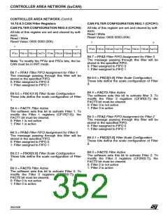
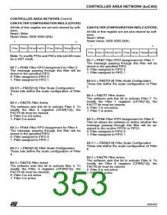
CAN FILTER CONFIGURATION REG.3 (CFCR3)
CONTROLLER AREA NETWORK (Cont’d)
CAN FILTER CONFIGURATION REG.2 (CFCR2)
All bits of this register are set and cleared by soft-
ware.
Read / Write
Reset Value: 0000 0000 (00h)
All bits of this register are set and cleared by soft-
ware.
Read / Write
Reset Value: 0000 0000 (00h)
7
0
7
0
FFA5 FSC51 FSC50 FACT5 FFA4 FSC41 FSC40 FACT4
FFA7 FSC71 FSC70 FACT7 FFA6 FSC61 FSC60 FACT6
Note: To modify FFAx and FSCx bits bxCAN must
be in INIT mode.
Bit 7 = FFA7 Filter FIFO Assignment for Filter 7
The message passing through this filter will be
stored in the specified FIFO.
Bit 7 = FFA5 Filter FIFO Assignment for Filter 5
The message passing through this filter will be
stored in the specified FIFO.
0: Filter assigned to FIFO 0
1: Filter assigned to FIFO 1
0: Filter assigned to FIFO 0
1: Filter assigned to FIFO 1
Bit 6:5 = FSC7[1:0] Filter Scale Configuration
These bits define the scale configuration of Filter
7.
Bit 6:5 = FSC5[1:0] Filter Scale Configuration
These bits define the scale configuration of Filter
5.
Bit 4 = FACT7 Filter Active
The software sets this bit to activate Filter 7. To
modify the Filter 7 registers (CF7R[7:0]), the
FACT7 bit must be cleared.
Bit 4 = FACT5 Filter Active
The software sets this bit to activate Filter 5. To
modify the filter 5 registers (CF5R[7:0]), the
FACT5 bit must be cleared.
0: Filter 5 is not active
1: Filter 5 is active
0: Filter 7 is not active.
1: Filter 7 is active.
Bit 3 = FFA6 Filter FIFO Assignment for Filter 6
This bit allows the software to define whether the
message passing through this filter will be as-
signed to the receive FIFO0 or FIFO1.
0: Filter assigned to FIFO 0
Bit 3 = FFA4 Filter FIFO Assignment for Filter 4
The message passing through this filter will be
stored in the specified FIFO.
0: Filter assigned to FIFO 0
1: Filter assigned to FIFO 1
1: Filter assigned to FIFO 1
Bit 2:1 = FSC6[1:0] Filter Scale Configuration
These bits define the scale configuration of Filter
6.
Bit 2:1 = FSC4[1:0] Filter Scale Configuration
These bits define the scale configuration of Filter
4.
Bit 0 = FACT6 Filter Active
The software sets this bit to activate Filter 6. To
modify the Filter 6 registers (CF6R[7:0]), the
FACT6 bit must be cleared.
Bit 0 = FACT4 Filter Active
The software sets this bit to activate filter 4. To
modify the Filter 4 registers (CF4R[7:0]), the
FACT4 bit must be cleared).
0: Filter 6 is not active
1: Filter 6 is active
0: Filter 4 is not active
1: Filter 4 is active
353/426
9

 STMICROELECTRONICS [ ST ]