CONTROLLER AREA NETWORK (bxCAN)
CONTROLLER AREA NETWORK (Cont’d)
10.10.8.3 CAN Filter Registers
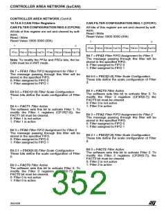
CAN FILTER CONFIGURATION REG.1 (CFCR1)
CAN FILTER CONFIGURATION REG.0 (CFCR0)
All bits of this register are set and cleared by soft-
ware.
All bits of this register are set and cleared by soft-
Read / Write
Reset Value: 0000 0000 (00h)
ware.
Read / Write
Reset Value: 0000 0000 (00h)
7
0
7
0
FFA3 FSC31 FSC30 FACT3 FFA2 FSC21 FSC20 FACT2
FFA1 FSC11 FSC10 FACT1 FFA0 FSC01 FSC00 FACT0
Bit 7 = FFA3 Filter FIFO Assignment for Filter 3
The message passing through this filter will be
stored in the specified FIFO.
Note: To modify the FFAx and FSCx bits, the bx-
CAN must be in INIT mode.
0: Filter assigned to FIFO 0
1: Filter assigned to FIFO 1
Bit 7 = FFA1 Filter FIFO Assignment for Filter 1
The message passing through this filter will be
stored in the specified FIFO.
Bit 6:5 = FSC3[1:0] Filter Scale Configuration
These bits define the scale configuration of Filter
3.
0: Filter assigned to FIFO 0
1: Filter assigned to FIFO 1
Bit 4 = FACT3 Filter Active
Bit 6:5 = FSC1[1:0] Filter Scale Configuration
The software sets this bit to activate filter 3. To
modify the Filter 3 registers (CF3R[0:7]) the
FACT3 bit must be cleared.
These bits define the scale configuration of Filter
1.
0: Filter 3 is not active
1: Filter 3 is active
Bit 4 = FACT1 Filter Active
The software sets this bit to activate Filter 1. To
modify the Filter 1 registers (CF1R[7:0]), the
FACT1 bit must be cleared.
Bit 3 = FFA2 Filter FIFO Assignment for Filter 2
The message passing through this filter will be
stored in the specified FIFO.
0: Filter 1 is not active
1: Filter 1 is active
0: Filter assigned to FIFO 0
1: Filter assigned to FIFO 1
Bit 3 = FFA0 Filter FIFO Assignment for Filter 0
The message passing through this filter will be
stored in the specified FIFO.
Bit 2:1 = FSC2[1:0] Filter Scale Configuration
These bits define the scale configuration of Filter
2.
0: Filter assigned to FIFO 0
1: Filter assigned to FIFO 1
Bit 0 = FACT2 Filter Active
Bit 2:1 = FSC0[1:0] Filter Scale Configuration
The software sets this bit to activate Filter 2. To
modify the Filter 2 registers (CF2R[0:7]), the
FACT2 bit must be cleared.
These bits define the scale configuration of Filter
0.
0: Filter 2 is not active
1: Filter 2 is active
Bit 0 = FACT0 Filter Active
The software sets this bit to activate Filter 0. To
modify the Filter 0 registers (CF0R[0:7]), the
FACT0 bit must be cleared.
0: Filter 0 is not active
1: Filter 0 is active
352/426
9

 STMICROELECTRONICS [ ST ]