CONTROLLER AREA NETWORK (bxCAN)
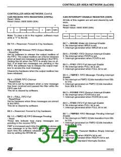
CAN INTERRUPT ENABLE REGISTER (CIER)
CONTROLLER AREA NETWORK (Cont’d)
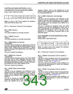
CAN RECEIVE FIFO REGISTERS (CRFRx)
Read / Write
Reset Value: 0000 0000 (00h)
All bits of this register are set and cleared by soft-
ware.
7
0
Read / Write
Reset Value: 0000 0000 (00h)
0
0
RFOM FOVR FULL
0
FMP1 FMP0
7
0
Note: To clear a bit in this register, software must
write a “1” to the bit.
WKUIE FOVIE1 FFIE1 FMPIE1 FOVIE0 FFIE0 FMPIE0 TMEIE
Bit 7 = WKUIE Wake-Up Interrupt Enable
0: No interrupt when WKUI is set.
1: Interrupt generated when WKUI bit is set.
Bit 7:6 = Reserved. Forced to 0 by hardware.
Bit 5 = RFOM Release FIFO Output Mailbox
- Read/Set
Bit 6 = FOVIE1 FIFO Overrun Interrupt Enable
0: No interrupt when FOVR is set.
Set by software to release the output mailbox of
the FIFO. The output mailbox can only be released
when at least one message is pending in the FIFO.
Setting this bit when the FIFO is empty has no ef-
fect. If at least two messages are pending in the
FIFO, the software has to release the output mail-
box to access the next message.
1: Interrupt generation when FOVR is set.
Bit 5 = FFIE1 FIFO Full Interrupt Enable
0: No interrupt when FULL bit is set.
1: Interrupt generated when FULL bit is set.
Cleared by hardware when the output mailbox has
been released.
Bit 4 = FMPIE1 FIFO Message Pending Interrupt
Enable
0: No interrupt on FMP[1:0] bits transition from 00b
to 01b.
Bit 4 = FOVR FIFO Overrun
- Read/Clear
This bit is set by hardware when a new message
has been received and passed the filter while the
FIFO was full.
1: Interrupt generated on FMP[1:0] bits transition
from 00b to 01b.
This bit is cleared by software.
Bit 3 = FOVIE0 FIFO Overrun Interrupt Enable
0: No interrupt when FOVR bit is set.
1: Interrupt generated when FOVR bit is set.
Bit 3 = FULL FIFO Full
- Read/Clear
Set by hardware when three messages are stored
in the FIFO.
This bit is cleared by software.
Bit 2 = FFIE0 FIFO Full Interrupt Enable
0: No interrupt when FULL bit is set.
1: Interrupt generated when FULL bit is set.
Bit 2 = Reserved. Forced to 0 by hardware.
Bit 1 = FMPIE0 FIFO Message Pending Interrupt
Enable
Bit 1:0 = FMP[1:0] FIFO Message Pending
- Read
These bits indicate how many messages are
pending in the receive FIFO.
0: No interrupt on FMP[1:0] bits transition from 00b
to 01b.
1: Interrupt generated on FMP[1:0] bits transition
from 00b to 01b.
FMP is increased each time the hardware stores a
new message in to the FIFO. FMP is decreased
each time the software releases the output mail-
box by setting the RFOM bit.
Bit 0 = TMEIE Transmit Mailbox Empty Interrupt
Enable
0: No interrupt when RQCPx bit is set.
1: Interrupt generated when RQCPx bit is set.
Note: refer to Standard Interrupts Section.
345/426
9

 STMICROELECTRONICS [ ST ]