J1850 Byte Level Protocol Decoder (JBLPD)
J1850 BYTE LEVEL PROTOCOL DECODER (Cont’d)
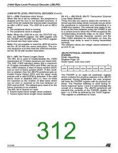
Bit 4 = SLP Receiver Sleep Mode.
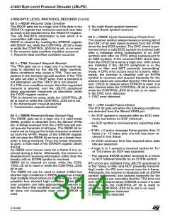
the end of a block of data. An interrupt request is
performed if the TRDY_M bit of the IMR register is
set. TEOBP should be reset by software in order to
avoid undesired interrupt routines, especially in in-
itialisation routine (after reset) and after entering
the End Of Block interrupt routine.
Writing “0” in this bit will cancel the interrupt re-
quest.
This bit is reset when the CONTROL.JDIS bit is
set at least for 6 MCU clock cycles (3 NOPs).
The SLP bit is written to one when the user pro-
gram does not want to receive any data from the
JBLPD VPWI pin until an EOFM symbol occurs.
This mode is usually set when a message is re-
ceived that the user does not require - including
messages that the JBLPD is transmitting.
If the JBLPD is not transmitting and is in Sleep
mode, no data is transferred to the RXDATA regis-
ter, the RDRF flag does not get set, and errors as-
sociated with received data (RDOF, CRCE, IFD,
IBD) do not get set. Also, the EODM flag will not
get set.
Note: When the TEOBP flag is set, the TXD_M bit
is reset by hardware.
Note: TEOBP can only be written to “0”.
If the JBLPD peripheral is transmitting and is in
sleep mode, no data is transferred to the RXDATA
register, the RDRF flag does not get set and the
RDOF error flag is inhibited. The CRCE, IFD, and
IBD flags, however, will NOT be inhibited while
transmitting in sleep mode.
The SLP bit cannot be written to zero by the user
program. The SLP bit is set on reset or TTO get-
ting set, and it will stay set upon JE getting set until
an EOFM symbol is received.
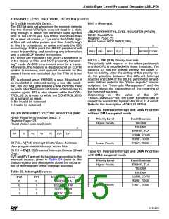
JBLPD INTERRUPT MASK REGISTER (IMR)
R250 - Read/Write
Register Page: 23
Reset Value: 0000 0000 (00h)
7
0
ERR_ TRDY_ RDRF_ TLA_ RXD_ EODM_ EOFM_ TXD_
M
M
M
M
M
M
M
M
The SLP gets cleared on reception of an EOF or a
Break symbol. SLP is set while CONTROL.JE is
reset and while CONTROL.JDIS is set.
To enable an interrupt source to produce an inter-
rupt request, the related mask bit must be set.
When these bits are reset, the related Interrupt
Pending bit can not generate an interrupt.
0: The JBLPD is not in Sleep Mode
1: The JBLPD is in Sleep Mode
Note: This register is forced to its reset value if the
CONTROL.JDIS bit is set at least for 6 clock cy-
cles (3 NOPs). If the JDIS bit is set for a shorter
time, the bits could be reset or not reset.
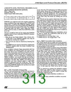
Bit 3:2 = Reserved.
Bit 1 = REOP Receiver DMA End Of Block Pend-
ing.
This bit is set after a receiver DMA cycle to mark
the end of a block of data. An interrupt request is
performed if the RDRF_M bit of the IMR register is
set. REOBP should be reset by software in order
to avoid undesired interrupt routines, especially in
initialisation routine (after reset) and after entering
the End Of Block interrupt routine.
Bit 7 = ERR_M Error Interrupt Mask bit.
This bit enables the “error” interrupt source to gen-
erate an interrupt request.
This bit is reset if the CONTROL.JDIS bit is set at
least for 6 clock cycles (3 NOPs).
0: Error interrupt source masked
1: Error interrupt source un-masked
Writing “0” in this bit will cancel the interrupt re-
quest.
This bit is reset when the CONTROL.JDIS bit is
set at least for 6 MCU clock cycles (3 NOPs).
Bit 6 = TRDY_M Transmit Ready Interrupt Mask
bit.
This bit enables the “transmit ready” interrupt
source to generate an interrupt request.
This bit is reset if the CONTROL.JDIS bit is set at
least for 6 clock cycles (3 NOPs).
Note: When the REOBP flag is set, the RXD_M bit
is reset by hardware.
Note: REOBP can only be written to “0”.
0: TRDY interrupt source masked
1: TRDY interrupt source un-masked
Bit 0 = TEOP Transmitter DMA End Of Block
Pending.
This bit is set after a transmitter DMA cycle to mark
316/426
9

 STMICROELECTRONICS [ ST ]