J1850 Byte Level Protocol Decoder (JBLPD)
J1850 BYTE LEVEL PROTOCOL DECODER (Cont’d)
Bit 0 = IBD Invalid Bit Detect.
Bit 0 = Reserved.
The IBD bit gets set whenever the receiver detects
that the filtered VPWI pin was not fixed in a state
long enough to reach the minimum valid symbol
time of Tv1 (or 35 µs). Any timing event less than
35 µs (and, of course, > 7 µs since the VPWI digit-
al filter will not allow pulses less than this through
its filter) is considered as noise and sets the IBD
accordingly. At this point the JBLPD peripheral will
cease transmitting and receiving any information
until a valid EOF symbol is received.
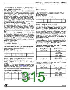
JBLPD PRIORITY LEVEL REGISTER (PRLR)
R249- Read/Write
Register Page: 23
Reset Value: 0001 0000 (10h)
7
0
PRL2 PRL1 PRL0 SLP
-
-
REOBP TEOBP
IBD errors are inhibited if the JBLPD peripheral is
in the “sleep or filter and NOT presently transmit-
ting” mode. An IBD error occurs once for a frame.
Afterwards, the receiver is disabled until an EOFM
symbol is received, and queued transmits for the
present frame are cancelled (but the TRA bit is not
set).
IBD is cleared when ERROR is read. Note that if
an invalid bit is detected during a bus idle condi-
tion, the IBD flag gets set and a new EOFmin must
be seen after the invalid bit before commencing to
receive again. IBD is also cleared while the CON-
TROL.JE bit is reset or while the CONTROL.JDIS
bit is set and on reset.
Bit 7:5 = PRL[2:0] Priority level bits
The priority with respect to the other peripherals
and the CPU is encoded with these three bits. The
value of “0” has the highest priority, the value “7”
has no priority. After the setting of this priority lev-
el, the priorities between the different Interrupt
sources and DMA of the JBLPD peripheral is hard-
ware defined (refer to the “Status register” bits de-
scription, the “Interrupts Management” and the
section about the explanation of the meaning of
the interrupt sources).
Depending on the value of the OP-
TIONS.DMASUSP bit, the DMA transfers can or
cannot be suspended by an ERROR or TLA event.
Refer to the description of DMASUSP bit.
0: No invalid bit detected
1: Invalid bit detected
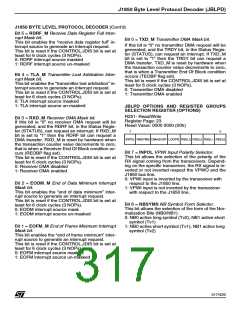
Table 60. Internal Interrupt and DMA Priorities
without DMA suspend mode
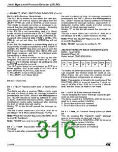
JBLPD INTERRUPT VECTOR REGISTER (IVR)
R248- Read/Write (except bits 2:1)
Register Page: 23
Priority Level
Event Sources
TX-DMA
Higher Priority
Reset Value: xxxx xxx0 (xxh)
RX-DMA
7
0
-
ERROR, TLA
EODM, EOFM
RDRF, REOB
TRDY, TEOB
V7
V6
V5
V4
V3
EV2
EV1
Bit 7:3 = V[7:3] Interrupt Vector Base Address.
User programmable interrupt vector bits.
Lower Priority
Bit 2:1 = EV[2:1] Encoded Interrupt Source (Read
Only).
EV2 and EV1 are set by hardware according to the
interrupt source, given in Table 59 (refer to the
Status register bits description about the explana-
tion of the meaning of the interrupt sources)
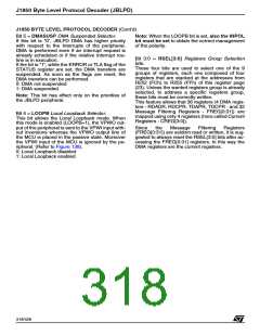
Table 61. Internal Interrupt and DMA Priorities
with DMA suspend mode
Priority Level
Event Sources
ERROR, TLA
TX-DMA
Higher Priority
Table 59. Interrupt Sources
RX-DMA
EODM, EOFM
RDRF, REOB
TRDY, TEOB
EV2
EV1
Interrupt Sources
ERROR, TLA
EODM, EOFM
RDRF, REOB
TRDY, TEOB
0
0
1
1
0
1
0
1
Lower Priority
315/426
9

 STMICROELECTRONICS [ ST ]