J1850 Byte Level Protocol Decoder (JBLPD)
J1850 BYTE LEVEL PROTOCOL DECODER (Cont’d)
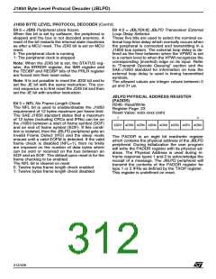
JBLPD ERROR REGISTER (ERROR)
R247- Read only
is set, then the TTO will timeout at 4000 prescaled
clock cycles. When the TTO flag is set then the di-
agnostic circuit will disable the VPWO signal, and
disable the JBLPD peripheral. The user program
must then clear the JE bit to remove the TTO error.
It can then retry the block by setting the JE bit
again.
Register Page: 23
Reset Value: 0000 0000 (00h)
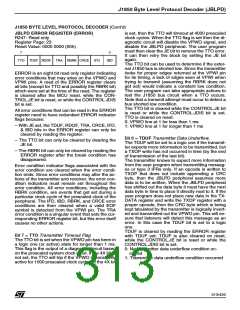
7
0
TTO TDUF RDOF TRA RBRK CRCE IFD
IBD
The TTO bit can be used to determine if the exter-
nal J1850 bus is shorted low. Since the transmitter
looks for proper edges returned at the VPWI pin
for its timing, a lack of edges seen at VPWI when
trying to transmit (assuming the RBRK does not
get set) would indicate a constant low condition.
The user program can take appropriate actions to
test the J1850 bus circuit when a TTO occurs.
Note that a transmit attempt must occur to detect a
bus shorted low condition.
The TTO bit is cleared while the CONTROL.JE bit
is reset or while the CONTROL.JDIS bit is set.
TTO is cleared on reset.
0: VPWO line at 1 for less than 1 ms
1: VPWO line at 1 for longer than 1 ms
ERROR is an eight bit read only register indicating
error conditions that may arise on the VPWO and
VPWI pins. A read of the ERROR register clears
all bits (except for TTO and possibly the RBRK bit)
which were set at the time of the read. The register
is cleared after the MCU reset, while the CON-
TROL.JE bit is reset, or while the CONTROL.JDIS
bit is set.
All error conditions that can be read in the ERROR
register need to have redundant ERROR indicator
flags because:
– With JE set, the TDUF, RDOF, TRA, CRCE, IFD,
& IBD bits in the ERROR register can only be
cleared by reading the register.
Bit 6 = TDUF Transmitter Data Underflow.
The TDUF will be set to a logic one if the transmit-
ter expects more information to be transmitted, but
a TXOP write has not occurred in time (by the end
of transmission of the last bit).
– The TTO bit can only be cleared by clearing the
JE bit.
– The RBRK bit can only be cleared by reading the
ERROR register after the break condition has
disappeared.
The transmitter knows to expect more information
from the user program when transmitting messag-
es or type 3 IFRs only. If an opcode is written to
TXOP that does not include appending a CRC
byte, then the JBLPD peripheral assumes more
data is to be written. When the JBLPD peripheral
has shifted out the data byte it must have the next
data byte in time to place it directly next to it. If the
user program does not place new data in the TX-
DATA register and write the TXOP register with a
proper opcode, then the CRC byte which is being
kept tabulated by the transmitter is logically invert-
ed and transmitted out the VPWO pin. This will en-
sure that listeners will detect this message as an
error. In this case the TDUF bit is set to a logic
one.
Error condition indicator flags associated with the
error condition are cleared when the error condi-
tion ends. Since error conditions may alter the ac-
tions of the transmitter and receiver, the error con-
dition indicators must remain set throughout the
error condition. All error conditions, including the
RBRK condition, are events that get set during a
particular clock cycle of the prescaled clock of the
peripheral. The IFD, IBD, RBRK, and CRCE error
conditions are then cleared when a valid EOF
symbol is detected from the VPWI pin. The TRA
error condition is a singular event that sets the cor-
responding ERROR register bit, but this error itself
causes no other actions.
TDUF is cleared by reading the ERROR register
with TDUF set. TDUF is also cleared on reset,
while the CONTROL.JE bit is reset or while the
CONTROL.JDIS bit is set.
0: No transmitter data underflow condition oc-
curred
1: Transmitter data underflow condition occurred
Bit 7 = TTO Transmitter Timeout Flag
The TTO bit is set when the VPWO pin has been in
a logic one (or active) state for longer than 1 ms.
This flag is the output of a diagnostic circuit based
on the prescaled system clock input. If the 4X bit is
not set, the TTO will trip if the VPWO is constantly
active for 1000 prescaled clock cycles. If the 4X bit
313/426
9

 STMICROELECTRONICS [ ST ]