J1850 Byte Level Protocol Decoder (JBLPD)
J1850 BYTE LEVEL PROTOCOL DECODER (Cont’d)
10.9.7.2 Stacked Registers
Register File) of the DMA receiver transaction
counter when the DMA between Peripheral and
Memory Space is selected. Otherwise, if the DMA
between Peripheral and Register File is selected,
this register points to a pair of registers that are
used as DMA Address register and DMA Transac-
tion Counter.
See the description of the OPTIONS register to
obtain more information on the map of the regis-
ters of this section.
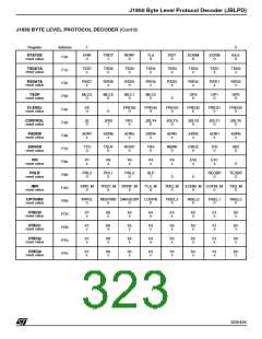
JBLPD RECEIVER DMA ADDRESS POINTER
REGISTER (RDAPR)
See Section 10.9.6.1and Section 10.9.6.2 for
more details on the use of this register.
R252 - RSEL[3:0]=0000b
Register Page: 23
Reset Value: xxxx xxxx (xxh)
Bit 0 = RF/MEM Receiver Register File/Memory
Selector.
7
0
If this bit is set to “1”, then the Register File will be
selected as Destination, otherwise the Memory
space will be used.
RA7
RA6
RA5
RA4
RA3
RA2
RA1
PS
0: Receiver DMA with Memory space
1: Receiver DMA with Register File
To select this register, the RSEL[3:0] bits of the
OPTIONS register must be reset
Bit 7:1 = RA[7:1] Receiver DMA Address Pointer.
RDAPR contains the address of the pointer (in the
Register File) of the Receiver DMA data source
when the DMA between the peripheral and the
Memory Space is selected. Otherwise, when the
DMA between the peripheral and Register File is
selected, this register has no meaning.
JBLPD TRANSMITTER DMA ADDRESS POINT-
ER REGISTER (TDAPR)
R254 - RSEL[3:0]=0000b
Register Page: 23
Reset Value: xxxx xxxx (xxh)
7
0
See Section 10.9.6.2 for more details on the use of
this register.
TA7
TA6
TA5
TA4
TA3
TA2
TA1
PS
Bit 0 = PS Memory Segment Pointer Selector.
This bit is set and cleared by software. It is only
meaningful if RDCPR.RF/MEM = 1.
0: The ISR register is used to extend the address
of data received by DMA (see MMU chapter)
1: The DMASR register is used to extend the ad-
dress of data received by DMA (see MMU chap-
ter)
To select this register, the RSEL[3:0] bits of the
OPTIONS register must be reset
Bit 7:1 = TA[7:1] Transmitter DMA Address Point-
er.
TDAPR contains the address of the pointer (in the
Register File) of the Transmitter DMA data source
when the DMA between the Memory Space and
the peripheral is selected. Otherwise, when the
DMA between Register File and the peripheral is
selected, this register has no meaning.
See Section 10.9.6.2 for more details on the use of
this register.
JBLPD RECEIVER DMA TRANSACTION
COUNTER REGISTER (RDCPR)
R253 - RSEL[3:0]=0000b
Register Page: 23
Reset Value: xxxx xxxx (xxh)
Bit 0 = PS Memory Segment Pointer Selector.
This bit is set and cleared by software. It is only
meaningful if TDCPR.RF/MEM = 1.
0: The ISR register is used to extend the address
of data transmitted by DMA (see MMU chapter)
1: The DMASR register is used to extend the ad-
dress of data transmitted by DMA (see MMU
chapter)
7
0
RC7
RC6
RC5
RC4
RC3
RC2
RC1 RF/MEM
To select this register, the RSEL[3:0] bits of the
OPTIONS register must be reset
Bit 7:1 = RC[7:1] Receiver DMA Counter Pointer.
RDCPR contains the address of the pointer (in the
320/426
9

 STMICROELECTRONICS [ ST ]