J1850 Byte Level Protocol Decoder (JBLPD)
J1850 BYTE LEVEL PROTOCOL DECODER (Cont’d)
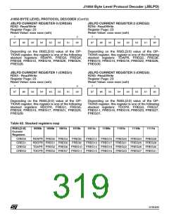
JBLPD CURRENT REGISTER 0 (CREG0)
R252- Read/Write
JBLPD CURRENT REGISTER 2 (CREG2)
R254- Read/Write
Register Page: 23
Register Page: 23
Reset Value: xxxx xxxx (xxh)
Reset Value: xxxx xxxx (xxh)
7
0
7
0
b7
b6
b5
b4
b3
b2
b1
b0
b7
b6
b5
b4
b3
b2
b1
b0
Depending on the RSEL[3:0] value of the OP-
TIONS register, this register is one of the following
stacked registers: RDAPR, FREG0, FREG4,
FREG8, FREG12, FREG16, FREG20, FREG24,
FREG28.
Depending on the RSEL[3:0] value of the OP-
TIONS register, this register is one of the following
stacked registers: TDAPR, FREG2, FREG6,
FREG10, FREG14, FREG18, FREG22, FREG26,
FREG30.
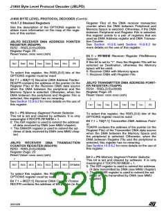
JBLPD CURRENT REGISTER 1 (CREG1)
R253 - Read/Write
JBLPD CURRENT REGISTER 3 (CREG3)
R255- Read/Write
Register Page: 23
Register Page: 23
Reset Value: xxxx xxxx (xxh)
Reset Value: xxxx xxxx (xxh)
7
0
7
0
b7
b6
b5
b4
b3
b2
b1
b0
b7
b6
b5
b4
b3
b2
b1
b0
Depending on the RSEL[3:0] value of the OP-
TIONS register, this register is one of the following
stacked registers: RDCPR, FREG1, FREG5,
FREG9, FREG13, FREG17, FREG21, FREG25,
FREG29.
Depending on the RSEL[3:0] value of the OP-
TIONS register, this register is one of the following
stacked registers: TDCPR, FREG3, FREG7,
FREG11, FREG15, FREG19, FREG23, FREG27,
FREG31.
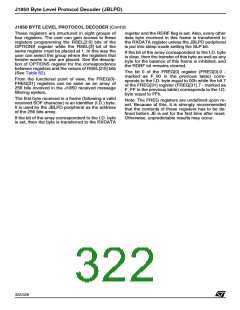
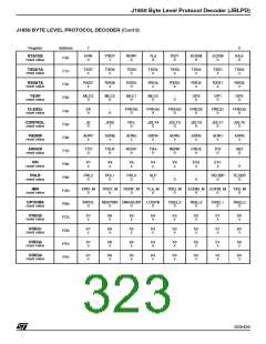
Table 62. Stacked registers map
RSEL[3:0]
Current
0000b
1000b
1001b
1010b
1011b
1100b
1101b
1110b
1111b
Registers
CREG0
CREG1
CREG2
CREG3
RDAPR FREG0 FREG4
RDCPR FREG1 FREG5
FREG8
FREG9
FREG12 FREG16 FREG20 FREG24 FREG28
FREG13 FREG17 FREG21 FREG25 FREG29
TDAPR FREG2 FREG6 FREG10 FREG14 FREG18 FREG22 FREG26 FREG30
TDCPR FREG3 FREG7 FREG11 FREG15 FREG19 FREG23 FREG27 FREG31
319/426
9

 STMICROELECTRONICS [ ST ]