J1850 Byte Level Protocol Decoder (JBLPD)
J1850 BYTE LEVEL PROTOCOL DECODER (Cont’d)
Bit 6 = JDIS Peripheral clock frozen.
When this bit is set by software, the peripheral is
stopped and the bus is not decoded anymore. A
reset of the bit restarts the internal state machines
as after a MCU reset. The JDIS bit is set on MCU
reset.
Bit 4:0 = JDLY[4:0] JBLPD Transceiver External
Loop Delay Selector.
These five bits are used to select the nominal ex-
ternal loop time delay which normally occurs when
the peripheral is connected and transmitting in a
J1850 bus system. The external loop delay is de-
fined as the time between when the VPWO is set
to a certain level to when the VPWI recognizes the
corresponding (inverted) edge on its input. Refer
to “Transmit Opcode Queuing” section and the
SAE-J1850 standard for information on how the
external loop delay is used in timing transmitted
symbols.
0: The peripheral clock is running
1: The peripheral clock is stopped
Note: When the JDIS bit is set, the STATUS reg-
ister, the ERROR register, the IMR register and
the TEOBP and REOBP bits of the PRLR register
are forced into their reset value.
Note: It is not possible to reset the JDIS bit and to
set the JE bit with the same instruction. The cor-
rect sequence is to first reset the JDIS bit and then
set the JE bit with another instruction.
The allowed values are integer values between 0
µs and 31 µs.
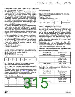
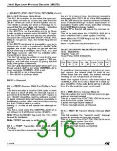
JBLPD PHYSICAL ADDRESS REGISTER
(PADDR)
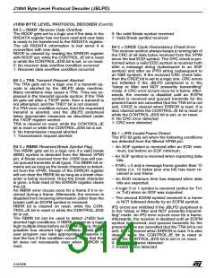
Bit 5 = NFL No Frame Length Check
R246- Read/Write
The NFL bit is used to enable/disable the J1850
requirement of 12 bytes maximum per frame limit.
The SAE J1850 standard states that a maximum
of 12 bytes (including CRCs and IFRs) can be on
the J1850 between a start of frame symbol (SOF)
and an end of frame symbol (EOF). If this condi-
tion is violated, then the JBLPD peripheral gets an
Invalid Frame Detect (IFD) and the sleep mode
ensues until a valid EOFM is detected. If the valid
frame check is disabled (NFL=1), then no limits
are imposed on the number of data bytes which
can be sent or received on the bus between an
SOF and an EOF. The default upon reset is for the
frame checking to be enabled.
Register Page: 23
Reset Value: xxxx xxxx (xxh)
7
0
ADR7 ADR6 ADR5 ADR4 ADR3 ADR2 ADR1 ADR0
The PADDR is an eight bit read/write register
which contains the physical address of the JBLPD
peripheral. During initialization the user program
will write the PADDR register with its physical ad-
dress. The Physical Address is used during in-
frame response types 1 and 2 to acknowledge the
receipt of a message. The JBLPD peripheral will
transmit the contents of the PADDR register for
type 1 or 2 IFRs as defined by the TXOP register.
This register is undefined on reset.
The NFL bit is cleared on reset
0: Twelve bytes frame length check enabled
1: Twelve bytes frame length check disabled
312/426
9

 STMICROELECTRONICS [ ST ]