J1850 Byte Level Protocol Decoder (JBLPD)
J1850 BYTE LEVEL PROTOCOL DECODER (Cont’d)
Bit 5 = DMASUSP DMA Suspended Selector.
If this bit is “0”, JBLPD DMA has higher priority
with respect to the Interrupts of the peripheral.
DMA is performed even if an interrupt request is
already scheduled or if the relative interrupt rou-
tine is in execution.
If the bit is “1”, while the ERROR or TLA flag of the
STATUS register are set, the DMA transfers are
suspended. As soon as the flags are reset, the
DMA transfers can be performed.
Note: When the LOOPB bit is set, also the INPOL
bit must be set to obtain the correct management
of the polarity.
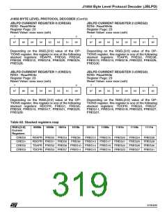
Bit 3:0 = RSEL[3:0] Registers Group Selection
bits.
These four bits are used to select one of the 9
groups of registers, each one composed of four
registers that are stacked at the addresses from
R252 (FCh) to R255 (FFh) of this register page
(23). Unless the wanted registers group is already
selected, to address a specific registers group,
these bits must be correctly written.
This feature allows that 36 registers (4 DMA regis-
ters - RDADR, RDCPR, TDAPR, TDCPR - and 32
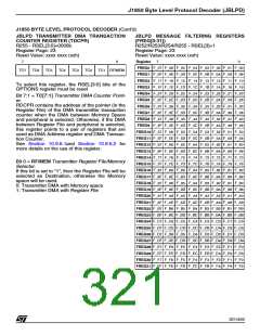
Message Filtering Registers - FREG[0:31]) are
mapped using only 4 registers (here called Current
Registers - CREG[3:0]).
0: DMA not suspended
1: DMA suspended
Note: This bit has effect only on the priorities of
the JBLPD peripheral.
Bit 4 = LOOPB Local Loopback Selector.
This bit allows the Local Loopback mode. When
this mode is enabled (LOOPB=1), the VPWO out-
put of the peripheral is sent to the VPWI input with-
out inversions whereas the VPWO output line of
the MCU is placed in the passive state. Moreover
the VPWI input of the MCU is ignored by the pe-
ripheral. (Refer to Figure 138).
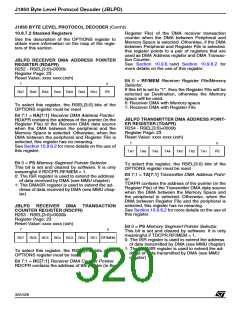
Since
the
Message
Filtering
Registers
(FREG[0:31]) are seldom read or written, it is sug-
gested to always reset the RSEL[3:0] bits after ac-
cessing the FREG[0:31] registers. In this way the
DMA registers are the current registers.
0: Local Loopback disabled
1: Local Loopback enabled
318/426
9

 STMICROELECTRONICS [ ST ]