J1850 Byte Level Protocol Decoder (JBLPD)
J1850 BYTE LEVEL PROTOCOL DECODER (Cont’d)
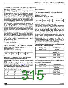
JBLPD SYSTEM FREQUENCY SELECTION
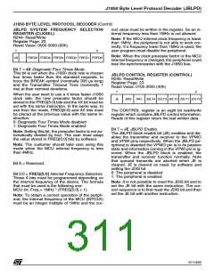
REGISTER (CLKSEL)
rect value must be written in the register. So an in-
ternal frequency less than 1MHz is not allowed.
R244- Read/Write
Note: If the MCU internal clock frequency is lower
than 1MHz, the peripheral is not able to work cor-
rectly. If a frequency lower than 1MHz is used, the
user program must disable the peripheral.
Register Page: 23
Reset Value: 0000 0000 (00h)
7
0
Note: When the clock prescaler factor or the MCU
internal frequency is changed, the peripheral could
lose the synchronization with the J1850 bus.
4X
-
FREQ5 FREQ4 FREQ3 FREQ2 FREQ1 FREQ0
Bit 7 = 4X Diagnostic Four Times Mode.
This bit is set when the J1850 clock rate is chosen
four times faster than the standard requests, to
force the BREAK symbol (nominally 300 µs long)
and the Transmitter Timeout Time (nominally 1
ms) at their nominal durations.
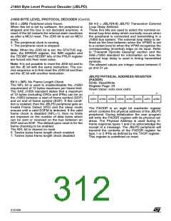
JBLPD CONTROL REGISTER (CONTROL)
R245- Read/Write
Register Page: 23
Reset Value: 0100 0000 (40h)
7
0
When the user want to use a 4 times faster J1850
clock rate, the new prescaler factor should be
stored in the FREQ[5:0] bits and the 4X bit must be
set with the same instruction. In the same way, to
exit from the mode, FREQ[5:0] and 4X bits must
be placed at the previous value with the same in-
struction.
JE
JDIS
NFL JDLY4 JDLY3 JDLY2 JDLY1 JDLY0
The CONTROL register is an eight bit read/write
register which contains JBLPD control information.
Reads of this register return the last written data.
0: Diagnostic Four Times Mode disabled
1: Diagnostic Four Times Mode enabled
Bit 7 = JE JBLPD Enable.
Note: Setting this bit, the prescaler factor is not au-
tomatically divided by four. The user must adapt
the value stored in FREQ[5:0] bits by software.
The JBLPD block enable bit (JE) enables and dis-
ables the transmitter and receiver to the VPWO
and VPWI pins respectively. When the JBLPD pe-
ripheral is disabled the VPWO pin is in its passive
state and information coming in the VPWI pin is ig-
nored. When the JBLPD block is enabled, the
transmitter and receiver function normally. Note
that queued transmits are aborted when JE is
cleared. JE is cleared on reset, by software and
setting the JDIS bit.
Note: The customer should take care using this
mode when the MCU internal frequency is less
than 4MHz.
Bit 6 = Reserved.
0: The peripheral is disabled
1: The peripheral is enabled
Bit 5:0 = FREQ[5:0] Internal Frequency Selectors.
These 6 bits must be programmed depending on
the internal frequency of the device. The formula
that must be used is the following one:
Note: It is not possible to reset the JDIS bit and to
set the JE bit with the same instruction. The cor-
rect sequence is to first reset the JDIS bit and then
set the JE bit with another instruction.
MCU Int. Freq.= 1MHz * (FREQ[5:0] + 1).
Note: To obtain a correct operation of the periph-
eral, the internal frequency of the MCU (INTCLK)
must be an integer multiple of 1MHz and the cor-
311/426
9

 STMICROELECTRONICS [ ST ]