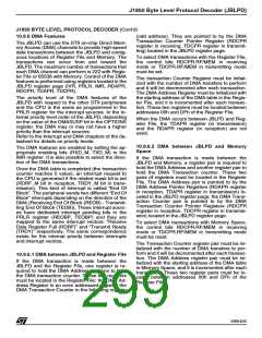
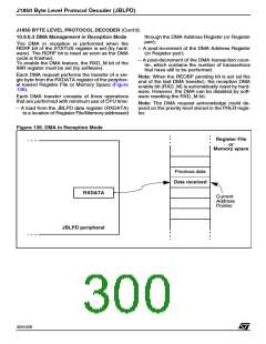
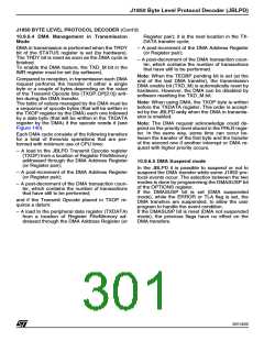
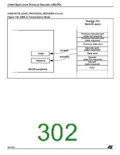
J1850 Byte Level Protocol Decoder (JBLPD)
J1850 BYTE LEVEL PROTOCOL DECODER (Cont’d)
10.9.7 Register Description
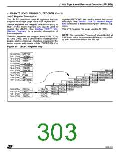
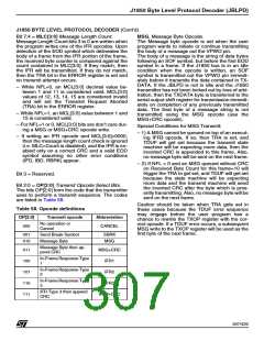
The JBLPD peripheral uses 48 registers that are
mapped in a single page of the ST9 register file.
register (OPTIONS) are used to select the current
sub-page. See Section 10.9.7.2 Stacked Regis-
ters section for a detailed description of these reg-
isters.
Twelve registers are mapped from R240 (F0h) to
R251 (FBh): these registers are usually used to
control the JBLPD. See Section 10.9.7.1 Un-
Stacked Registers for a detailed description of
these registers.
The ST9 Register File page used is 23 (17h).
NOTE: Bits marked as “Reserved” should be left at
their reset value to guarantee software compatibil-
ity with future versions of the JBLPD.
Thirty-six registers are mapped from R252 (FCh)
to R255 (FFh). This is obtained by creating 9 sub-
pages, each containing 4 registers, mapped in the
same register addresses; 4 bits (RSEL[3:0]) of a
Figure 141. JBLPD Register Map
R240 (F0h) STATUS
R241 (F1h) TXDATA
R242 (F2h) RXDATA
TXOP
R243 (F3h)
R244 (F4h) CLKSEL
R245 (F5h) CONTROL
R246 (F6h) PADDR
R247 (F7h) ERROR
R248 (F8h) IVR
FREG28
FREG24FREG29
R249 (F9h) PRLR
R250 (FAh) IMR
R251 (FBh) OPTIONS
FREG20FREG25FREG30
FREG16FREG21FREG26FREG31
FREG12FREG17FREG22FREG27
FREG8 FREG13FREG18FREG23
FREG4 FREG9 FREG14FREG19
FREG0 FREG5 FREG10FREG15
FREG1 FREG6 FREG11
R252 (FCh) CREG0
R253 (FDh) CREG1
R254 (FEh) CREG2
R255 (FFh) CREG3
RDAPR
RDCPR
TDAPR
TDCPR
FREG2 FREG7
FREG3
303/426
9

 STMICROELECTRONICS [ ST ]