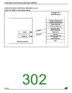
J1850 Byte Level Protocol Decoder (JBLPD)
J1850 BYTE LEVEL PROTOCOL DECODER (Cont’d)
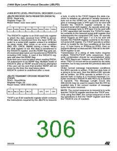
JBLPD RECEIVE DATA REGISTER (RXDATA)
R242- Read only
a byte. A write to the TXOP triggers the state ma-
chine to initialize an attempt to serially transmit a
byte out on the VPWO pin. An opcode which trig-
gers a message byte or IFR type 3 to be sent will
transfer the TXDATA register contents to the
transmit serial shift register. An opcode which trig-
gers a message byte or IFR type 3 to be sent with
a CRC appended will transfer the TXDATA regis-
ter contents to the transmit serial shift register and
subsequently the computed CRC byte. An opcode
which triggers an IFR type 1 or 2 to be sent will
transfer the PADDR register contents to the trans-
mit serial shift register. If a TXOP opcode is written
which is invalid for the bus conditions at the time
(e.g. 12 byte frame or IFR3ing an IFR2), then no
transmit attempt is tried and the TRA bit in the ER-
ROR register is set.
Transmission of a string of data bytes requires
multiple TXDATA/TXOP write sequences. Each
write combination should be accomplished while
the TRDY flag is set. However, writes to the TXOP
when TRDY is not set will be accepted by the state
machine, but it may override the previous data and
opcode.
Under normal message transmission conditions
the MSG opcode is written. If the last data byte of
a string is to be sent, then the MSG+CRC opcode
will be written. An IFRx opcode is written if a re-
sponse byte or bytes to a received message (i.e.
bytes received in RXDATA with RDT=0) is wanted
to transmit. The Message Length Count bits
(MLC[3:0]) may be used to require that the IFR be
enabled only if the correct number of message
bytes has been received.
Register Page: 23
Reset Value: xxxx xxxx (xxh)
7
0
RXD7 RXD6 RXD5 RXD4 RXD3 RXD2 RXD1 RXD0
The RXDATA register is an 8-bit read only register
in which the data received from VPWI is stored.
VPWI data is transferred from the input VPW de-
coder to a serial shift register unless it is inhibited
by sleep mode, filter mode or an error condition
(IBD, IFD, CRCE, RBRK) during a frame. When
the shift register is full, this data is transferred to
the RXDATA register, and the RDRF flag gets set.
All received data bytes are transferred to RXDATA
including CRC bytes. A read of the RXDATA reg-
ister will clear the RDRF flag.
Note that care must be taken when reading RXDA-
TA subsequent to an RDRF flag. Multiple reads of
RXDATA after an RDRF should only be attempted
if the user can be sure that another RDRF will not
occur by the time the read takes place.
RXDATA content is undefined after a reset.
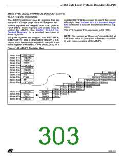
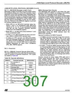
JBLPD TRANSMIT OPCODE REGISTER
(TXOP)
R243 - Read/Write
Register Page: 23
Reset Value: 0000 0000 (00h)
7
0
NOTE: The correct sequence to transmit is to write
first the TXDATA register and then the TXOP one.
Only using the DMA, the correct sequence of writ-
ing operations is first the TXOP register and then
the TXDATA one (if needed).
MLC3 MLC2 MLC1 MLC0
-
OP2
OP1
OP0
TXOP is an 8-bit read/write register which contains
the instructions required by the JBLPD to transmit
306/426
9

 STMICROELECTRONICS [ ST ]